
Layout for semiconductor device and method of fabricating the semiconductor device

a semiconductor device and semiconductor technology, applied in the field of semiconductor devices and methods of fabricating semiconductor devices, can solve the problems of severe noise generation between lines, reduced yield, and restriction of dram capacity, and achieve the effect of preventing the sac failure of the storage node and increasing the cell density

Active Publication Date: 2013-03-12
SK HYNIX INC
View PDF9 Cites 14 Cited by
  • Summary
  • Abstract
  • Description
  • Claims
  • Application Information

AI Technical Summary

Benefits of technology

The present invention provides a layout for a semiconductor device that allows for a larger number of capacitors in the same area, resulting in increased cell density and the ability to obtain more semiconductor chips from a wafer. The layout includes active regions, device isolation films, bit lines, and word lines with a number of improvements such as an inclined portion with a bit-line contact region, and a longer distance between bit lines to prevent failure. A method of fabricating the semiconductor device is also provided facilitating patterning of the active region and the formation of a storage node contact.

Problems solved by technology

However, a is size limit on the chip has placed a constraint on the increase of the DRAM capacity.
When the chip size increases the number of chips per wafer should decrease, leading to the reduction in yield.
In case of the 4F2 layout, however, the active regions should be formed in a cylindrical shape, a vertical type gate should be used, and a severe noise is generated between the lines.
Thus, the 4F2 layout has many problems yet to be solved down the road before mass production.

Method used


Image

  • Layout for semiconductor device and method of fabricating the semiconductor device
  • Layout for semiconductor device and method of fabricating the semiconductor device
  • Layout for semiconductor device and method of fabricating the semiconductor device

Examples


Embodiment Construction

[0027]An exemplary embodiment of a layout for a semiconductor device is according to the present invention and a method of fabricating the semiconductor device will now be described in greater detail with reference to the accompanying drawings.

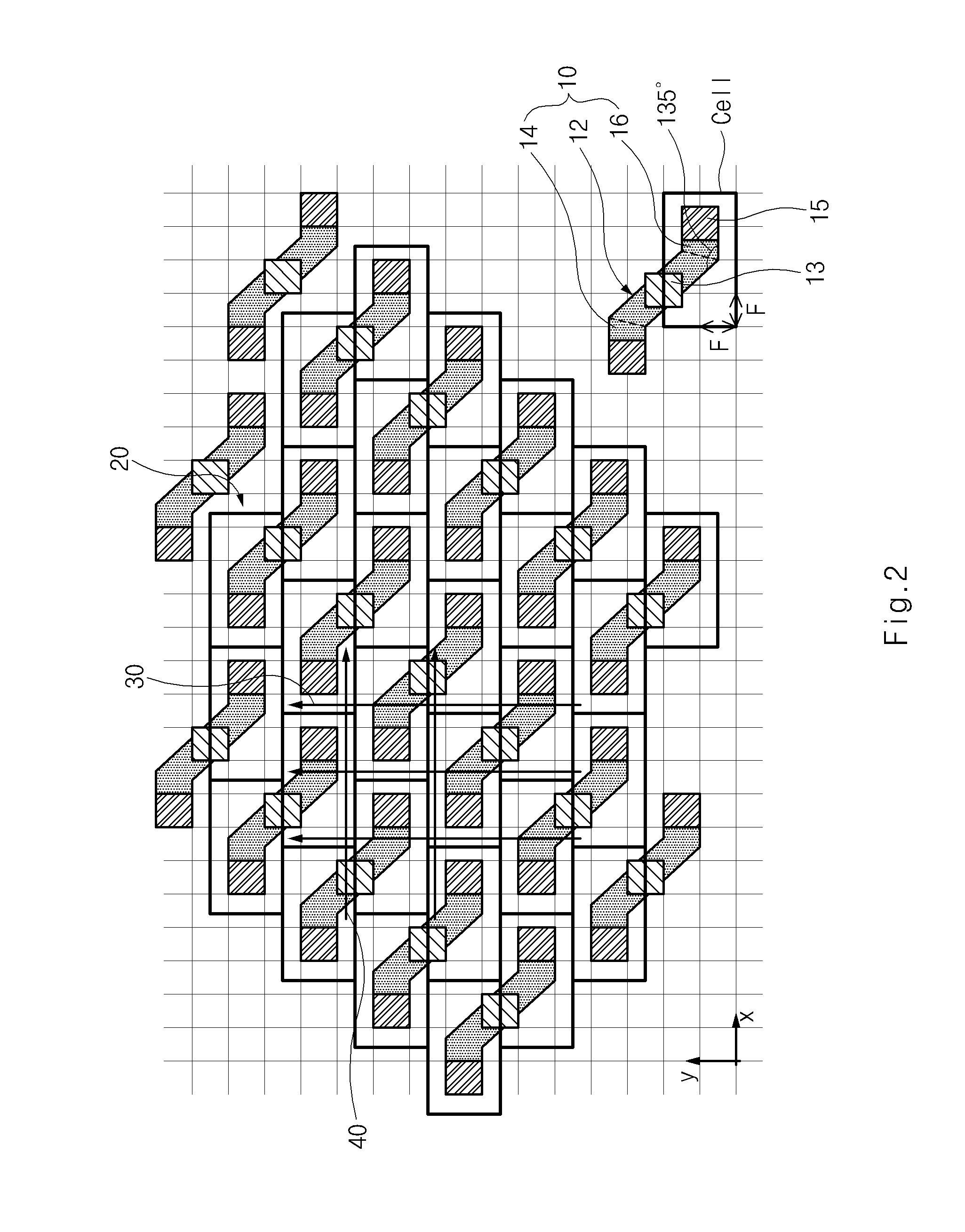
[0028]FIG. 2 to FIG. 4 show a layout for a semiconductor device according to one embodiment of the present invention. An active region 10 shown in FIG. 2 to FIG. 4 has substantially the same configuration and structure. One difference is that the layout arrangement of active regions 10 around a device isolation film 20 differs from one another. The layout shown in FIG. 2 illustrates the 8F2 layout, the layout shown in FIG. 3 illustrates the 6F2 layout, and the layout shown in FIG. 4 illustrates the 5.5F2 layout.

[0029]In the following, a common construction among the active regions 10 in FIG. 2 to FIG. 4 will first be explained, followed by the layout arrangement of each active region 10 and a method thereof in order.

[0030]Each active region 10...


PUM


Abstract

In a layout for a semiconductor device, each active region comprises a first active region, a right active region on the right side of the first active region, a left active region on the left side of the first active region, an upper active region on the upper side of the first active region and a lower active region on the lower side of the first active region, wherein the first active region, the right active region, the left active region, the upper active region and the lower active region each have an inclined portion having a bit-line contact region; and first and second portions having a storage node contact region, first and second ends formed on left and right ends of the inclined portion at a predetermined tilt angle with respect to the inclined portion, the active region being intersected by two word lines and one bit line.

Description

CROSS-REFERENCE TO RELATED APPLICATION[0001]The present application claims priority to Korean patent application number 10-2009-70476, filed on 31 Jul. 2009, which is incorporated by reference in its entirety.BACKGROUND OF THE INVENTION[0002]The present invention relates to a semiconductor device and a method of fabricating the semiconductor device. More particularly, the present invention relates to a layout arrangement and design for active regions and device isolation films of a semiconductor device, and to a method of fabricating the semiconductor device having the layout.[0003]In recent years, there has been an increasing demand for large-capacity DRAMs (Dynamic Random Access Memories). However, a is size limit on the chip has placed a constraint on the increase of the DRAM capacity. When the chip size increases the number of chips per wafer should decrease, leading to the reduction in yield. Accordingly, great efforts have been made to change the cell layout so as to reduce th...

Claims


Application Information

Patent Timeline
Patent Type & Authority Patents(United States)
IPC IPC(8): H01L21/82H01L29/94H01L27/108H01L23/52H01L21/44H10B12/00
CPCH01L27/10882H01L27/0207H10B12/48G03F7/70425G03F7/70433G03F7/70475
Inventor LEE, HO HYUK
Owner SK HYNIX INC
Learn More