Electronic component, and a method of manufacturing an electronic component

a manufacturing method and electronic technology, applied in the field of electronic components, can solve the problems of a1 may be problematic, flash memory scaling to lower dimensions has become a real problem, and the demand of a high value of an electric current required for switching between a crystalline phase and an amorphous phase, so as to increase the dissipated power density, reduce the programming current, and increase the set resistance

Active Publication Date: 2013-01-22
NXP BV
View PDF10 Cites 2 Cited by
  • Summary
  • Abstract
  • Description
  • Claims
  • Application Information

AI Technical Summary

Benefits of technology

[0020]According to an exemplary embodiment of the invention, small islands of a phase change material may be embedded in an electrically insulating matrix to form a conductive part with a high value of the resistivity. As an upper bound of the resistance for exemplary embodiments of the invention, it may be added: Rmatrix>Rcryst.path and / or ρmatrix>ρcryst.path. In practice it may be appropriate if Rmatrix>Ramorphous.path and / or ρmatrix>ρamorphous.path, but this is not a strict limit and thus optionally for the first criterion. For the situation that Rcryst.path<Rmatrix<Ramorphous.path. a structure is obtained which resembles a parallel heater line, see WO 2004 / 057676. Thus, the electric programming current necessary for switching the consecutive phase change material islands between a crystalline and an amorphous phase may be reduced, when the programming power is maintained constant. Alternatively, with a constant programming current, the programming power may be reduced. This may allow for a miniature manufacture of electronic components such as memory cells, thereby increasing the integration density of memory cells in a memory array. This is due to the fact that the necessary programming current / power is a limiting factor in reducing the size of phase change material based electronic driving circuitry components.
[0037]A number of molecules (or a concentration, a volume percentage, or a weight percentage) of the plurality of islands may be smaller than a number of molecules (or a concentration, a volume percentage, or a weight percentage) of the matrix, particularly may be up to four times smaller than a number of molecules of the matrix. By adjusting the relative concentration of matrix material and island material, the conductivity and the self-organization properties may be accurately adjusted.

Problems solved by technology

In the field of non-volatile memories, flash memory scaling to lower dimensions has become a real issue.
However, the demand of a high value of an electric current required for switching between a crystalline phase and an amorphous phase according to US 2005 / 0212024 A1 may be problematic.

Method used


Image

  • Electronic component, and a method of manufacturing an electronic component
  • Electronic component, and a method of manufacturing an electronic component
  • Electronic component, and a method of manufacturing an electronic component

Examples


Embodiment Construction

[0056]The illustration in the drawing is schematical. In different drawings, similar or identical elements are provided with the same reference signs.

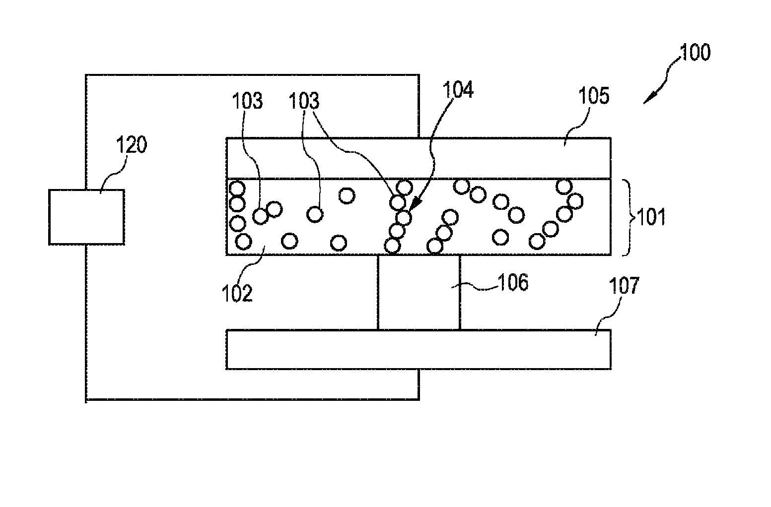
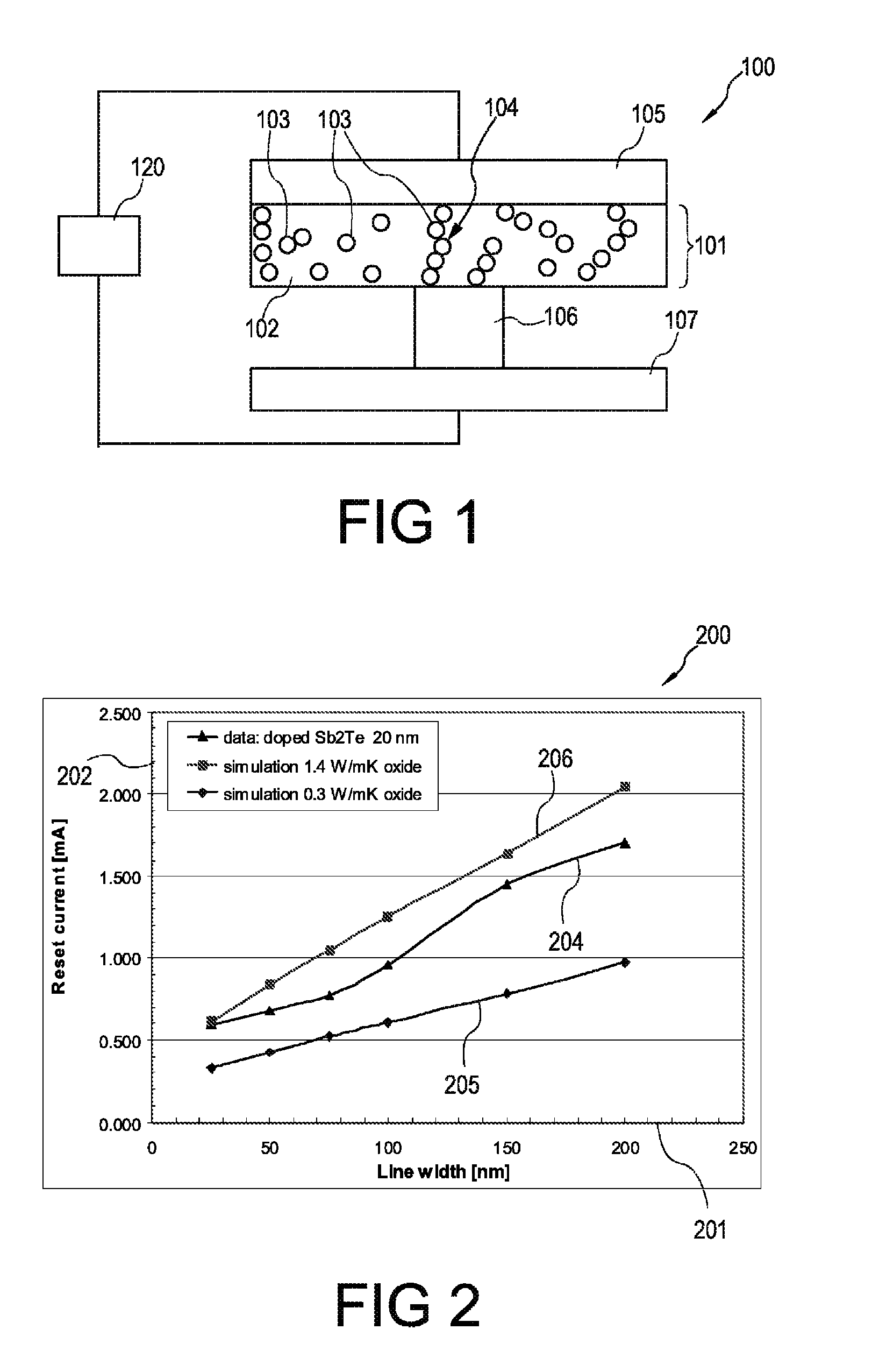
[0057]In the following, referring to FIG. 1, a memory cell 100 according to an exemplary embodiment of the invention will be explained.

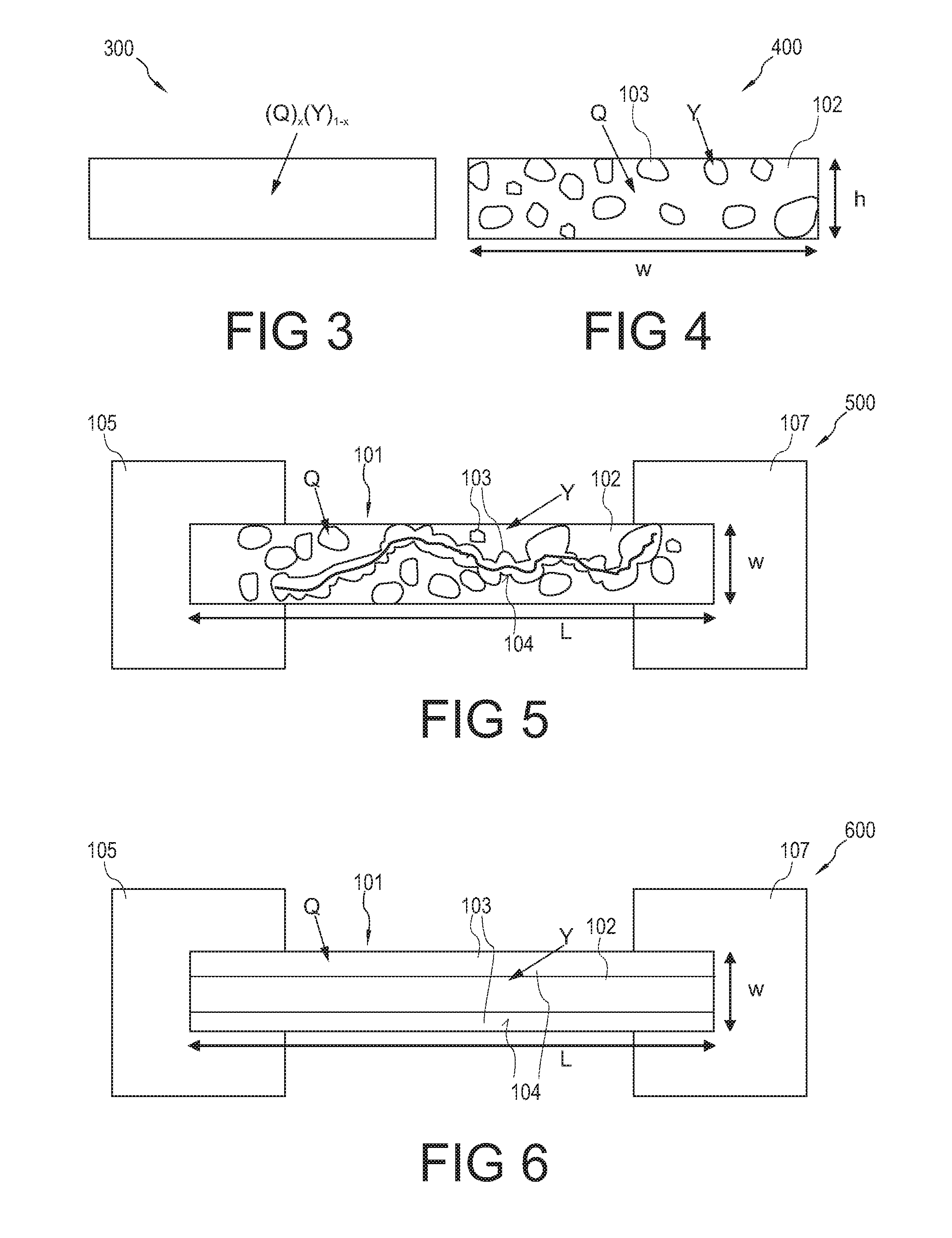
[0058]The memory cell 100 comprises a phase change film 101 consisting of a matrix 102 of a single (exactly one) electrically insulating material and a number of phase change material islands 103 embedded in the matrix 102 and comprising a single (exactly one) phase change material which is convertible between a crystalline phase and an amorphous phase having different electrical properties. As can be taken from FIG. 1, in a central part of the phase change line cell 101, a plurality of the islands 103 form a continuous (percolation) path 104 allowing the conductance of an electric current between a first electrode 105 and an electrically conductive spatially narrow contact element 106 which is electric...


PUM


Abstract

An electronic component (100) comprising a matrix (102) and a plurality of islands (103) embedded in the matrix (102) and comprising a material which is convertible between at least two states characterized by different electrical properties, wherein the plurality of islands (103) form a continuous path (104) in the matrix (102).

Description

FIELD OF THE INVENTION[0001]The invention relates to an electronic component.[0002]Moreover, the invention relates to a method of manufacturing an electronic component.BACKGROUND OF THE INVENTION[0003]In the field of non-volatile memories, flash memory scaling to lower dimensions has become a real issue. Technologies to face this challenge are ferroelectric, magnetic and phase change memories, the latter one being promising for the replacement of flash and showing characteristics that may allow replacement of other types of memories such as DRAM. Phase change memories are a possible solution for the unified memory being an important step in the electronics art. OTP (“on time programmable”) and MTP (“multiple times programmable”) memories open a field that may present a great opportunity for phase change memories as well.[0004]Phase change memories are based on a reversible memory switching using, for instance, chalcogenide materials. The ability of these materials to undergo fast ph...

Claims


Application Information

Patent Timeline
Patent Type & Authority Patents(United States)
IPC IPC(8): H01L47/00
CPCH01L45/06H01L45/1246H01L45/144H01L45/1608H10N70/231H10N70/828H10N70/8828H10N70/021
Inventor JEDEMA, FRISO JACOBUS
Owner NXP BV
Why Eureka
Try Eureka