Eureka AIR delivers breakthrough ideas for toughest innovation challenges, trusted by R&D personnel around the world.

Integrated method for high-density interconnection of electronic components through stretchable interconnects

a technology of stretchable electronics and integrated methods, which is applied in the direction of resistive material coating, cable/conductor manufacturing, solid-state devices, etc., can solve the problems of conventional interconnection and bonding methods, etc., and cannot be applied to pdms-based stretchable electronics. , to achieve the effect of high bonding density, simple and integrated process, and resistance to mechanical deformation

Inactive Publication Date: 2013-01-08
GUO LIANG +1
View PDF22 Cites 19 Cited by
  • Summary
  • Abstract
  • Description
  • Claims
  • Application Information

AI Technical Summary

Benefits of technology

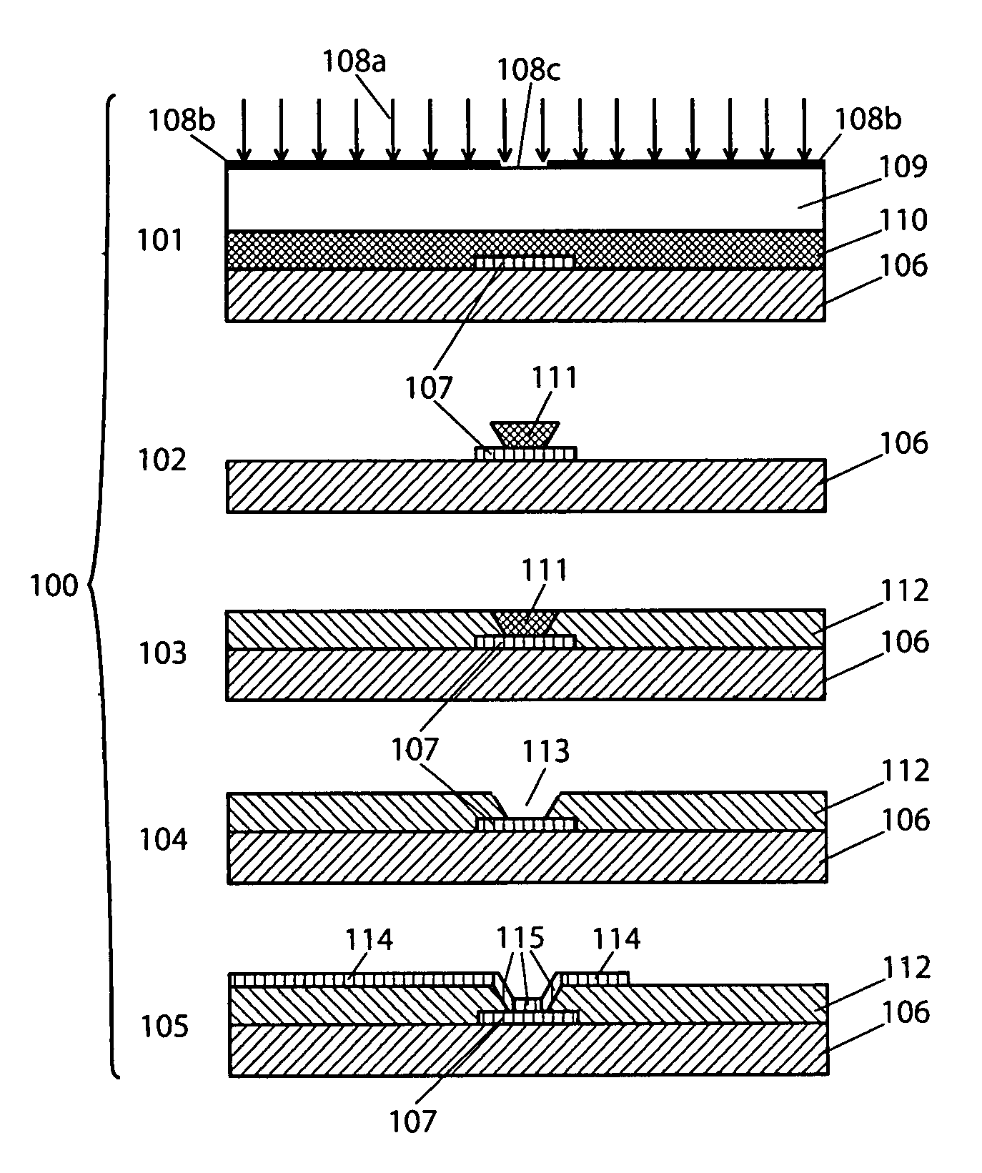
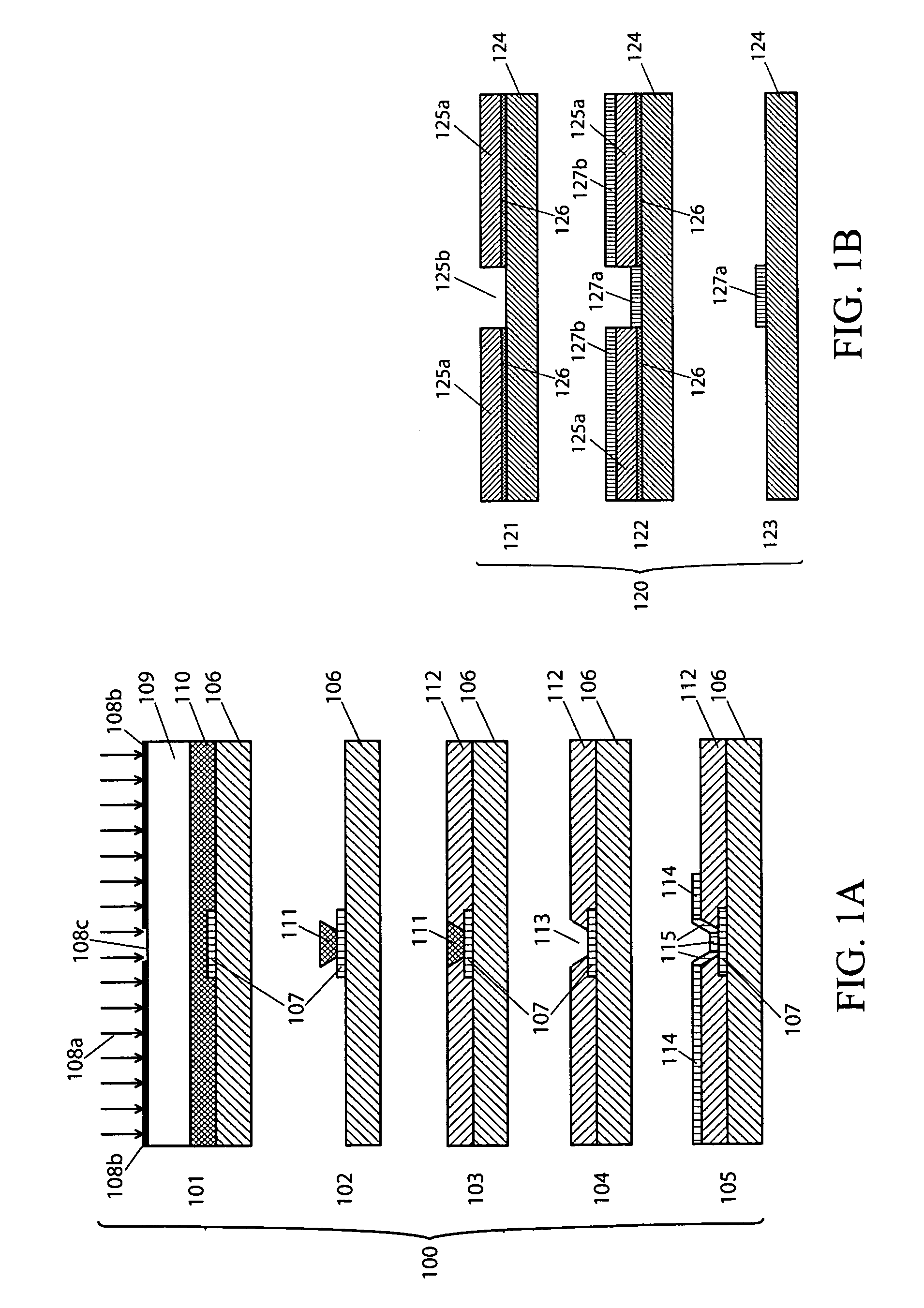
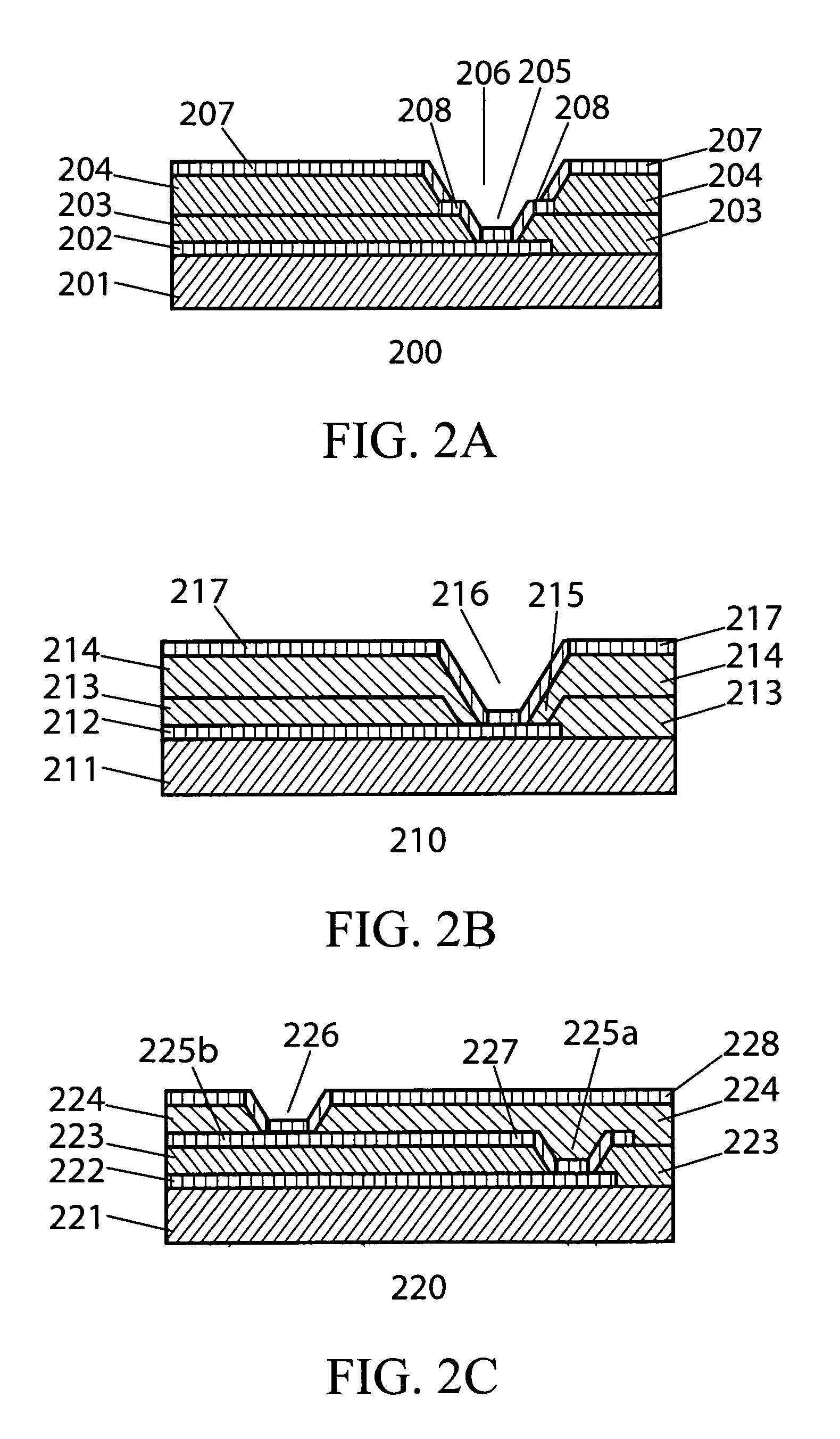
[0012]The unique features that differentiate the present invention from the prior arts are: (1) the fabrication method pertains to an elastomeric substrate system; (2) the method is a simple and integrated process in align with the fabrication of multilayer interconnects on PDMS substrates; (3) the density of the achieved bonding is very high; (4) the via-bonds is strong, reliable and resistant to mechanical deformations; (5) the via-bonds occupy a very small area as compared to other bonding methods applied to a PDMS-based system; (6) the via-bonding process is in low temperature (no more than 90° C.) and CMOS compatible; (7) the process is biocompatible and the resulting microelectrode array systems are suitable for implantation.

Problems solved by technology

Owing to the viscoelastic nature of the PDMS material, conventional interconnection and bonding methods as used with other substrate materials (e.g., silicon, parylene, polyimide, FR4, etc.) are not applicable to PDMS-based stretchable electronics, particularly when a high I / O count electronic component, such as a PDMS-based retinal electrode array, is involved.

Method used


Image

  • Integrated method for high-density interconnection of electronic components through stretchable interconnects
  • Integrated method for high-density interconnection of electronic components through stretchable interconnects
  • Integrated method for high-density interconnection of electronic components through stretchable interconnects

Examples


Embodiment Construction

[0025]At present, PDMS is the softest material that has been used as the fabrication substrate. While its low Young's modulus makes it advantageous in applications where large mechanical deformation of the device is necessary, where an intimate contact to a curved surface is needed, and where mechanical impedance matching to the surrounding soft tissues is desired, however, its low Young's modulus, high coefficient of thermal expansion (more than 100 times than that of silicon), poor adhesion to other microfabrication materials, and porous bulk structure, make the electronic fabrication using PDMS as the substrate extremely challenging, particularly when a high-density electronic system is desired. Most conventional microfabrication techniques that work favorably with other substrate materials, including silicon and other polymers, fail to work when transferred to PDMS-based fabrication. As a result, the integration density and capacity of PDMS-based electronic systems have been low...


PUM

PropertyMeasurementUnit
Young's modulusaaaaaaaaaa
areaaaaaaaaaaa

Abstract

Stretchable multi-chip modules (SMCMs) are capable of withstanding large mechanical deformations and conforming to curved surfaces. These SMCMs may find their utilities in elastic consumer electronics such as elastic displays, skin-like electronic sensors, etc. In particular, stretchable neural implants provide improved performances as to cause less mechanical stress and thus fewer traumas to surrounding soft tissues. Such SMCMs usually comprise of various electronic components attached to or embedded in a polydimethylsiloxane (PDMS) substrate and wired through stretchable interconnects. However, reliably and compactly connecting the electronic components to PDMS-based stretchable interconnects is very challenging. This invention describes an integrated method for high-density interconnection of electronic components through stretchable interconnects in an SMCM. This invention has applications in high-density SMCMs, as well as high-density stretchable / conformable neural interfaces.

Description

CROSS-REFERENCE TO RELATED APPLICATIONS[0001]This application claims the benefit of U.S. Provisional Patent Application No. 61 / 322,110 filed Apr. 8, 2010 and titled “Fabrication of Multilayer Wiring Interconnects on PDMS Substrate”, incorporated herein by reference.STATEMENT REGARDING FEDERALLY SPONSORED RESEARCH OR DEVELOPMENT[0002]This invention was made with government support under Grant No. R01-EB006179 awarded by the National Institutes of Health. The government has certain rights in the invention.REFERENCE TO SEQUENCE LISTING, A TABLE, OR A COMPUTER PROGRAM LISTING COMPACT DISC APPENDIX[0003](Not Applicable)BACKGROUND OF THE INVENTION[0004]1. Field of Endeavor[0005]The present invention relates generally to electronics interconnection and packaging, and more particularly, the invention relates to the wiring and packaging of stretchable multi-chip modules (SMCMs), including the wiring and packaging of high-density polydimethylsiloxane (PDMS)-based stretchable microelectrode ar...

Claims


Application Information

Patent Timeline
Patent Type & Authority Patents(United States)
IPC IPC(8): H01L21/4763
CPCH01L23/5387H01L23/5389H01L24/19H01L24/20H05K1/0283H05K3/4644A61N1/0543H01L25/0652H01L2224/04105H01L2924/01013H01L2924/01079H05K1/185H05K3/4691H05K2201/09509H01L2924/01005H01L2924/01006H01L2924/01019H01L2924/01024H01L2924/01033H01L2924/01074H01L2924/01077H01L2924/01078H01L2924/10253H01L2924/00H01L2924/14
Inventor GUO, LIANGDEWEERTH, STEPHEN P.
Owner GUO LIANG
Why Eureka
Eureka Blog
Learn More