
Memory embedded logic semiconductor device having memory region and logic circuit region

a technology of logic circuit and memory region, which is applied in the direction of semiconductor devices, basic electric elements, electrical appliances, etc., can solve the problems of increased connection resistance, high manufacturing cost, and difficulty in thinning down, so as to reduce the connection resistance between the capacitor and the first diffusion region of the cell transistor, prevent short circuit, and reduce the effect of manufacturing cos

Inactive Publication Date: 2012-08-28
RENESAS ELECTRONICS CORP
View PDF15 Cites 6 Cited by
  • Summary
  • Abstract
  • Description
  • Claims
  • Application Information

AI Technical Summary

Benefits of technology

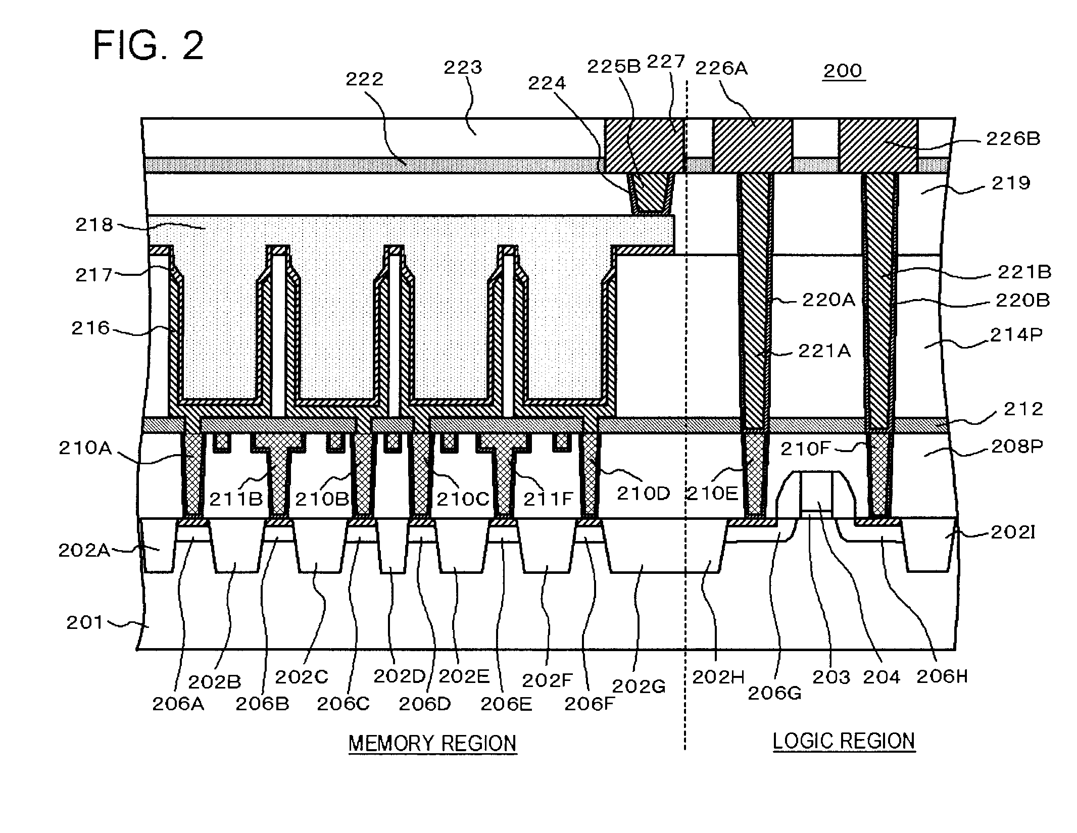
[0016]As described above, in the method of manufacturing the semiconductor device according to the invention, the first contact hole reaching the first diffusion region of the cell transistor, the bit line contact hole reaching the second diffusion region of the cell transistor, and the interconnect groove communicating with the bit line contact hole are buried in the same insulating film (first insulating film), and the first contact plug, the bit line contact plug and the bit line are respectively formed by burying the conductive materials in the first contact hole, the bit line contact hole and the interconnect groove. Further, in the manufacturing method, the first contact plug is electrically connected to the capacitor formed in the third insulating film on the second insulating film through the first opening formed in the second insulating film. Hereby, the distance between the capacitor and the first diffusion region of the cell transistor may be shortened, to thereby allow the connection resistance between the capacitor and the cell transistor to be lowered.
[0017]In addition, since the aspect ratio of the first contact hole is relatively small, it is possible to secure sufficient connection resistance even when the size (opening diameter) of the first opening is reduced. For this reason, it is possible to prevent short circuit between the conductive material within the first opening and the bit line by reducing the size (opening diameter) of the first opening.
[0018]In addition, the first contact plug and the bit line may be simultaneously formed by simultaneously burying the conductive materials in the first contact hole and the interconnect groove, to thereby allow the number of processes to be reduced.
[0020]As described above, in the semiconductor device according to the invention, any of the bit line contact plug, the bit line and the first contact plug is buried in the first insulating film, and the first contact plug is electrically connected to the capacitor within the third insulating film through the first through hole formed in the second insulating film. Therefore, the distance between the capacitor and the first diffusion region of the cell transistor may be shortened, to thereby allow the connection resistance between the capacitor and the cell transistor to be lowered.
[0021]In addition, since the aspect ratio of the first contact hole is relatively small, it is possible to secure sufficient connection resistance even when the size (opening diameter) of the first opening is reduced. For this reason, it is possible to prevent short circuit between the first opening and the bit line by reducing the size (opening diameter) of the first opening.
[0022]According to the invention, it is possible to lower the connection resistance between the capacitor and the cell transistor. In addition, it is possible to suppress the cost of manufacturing the semiconductor device by reducing the number of manufacturing processes.

Problems solved by technology

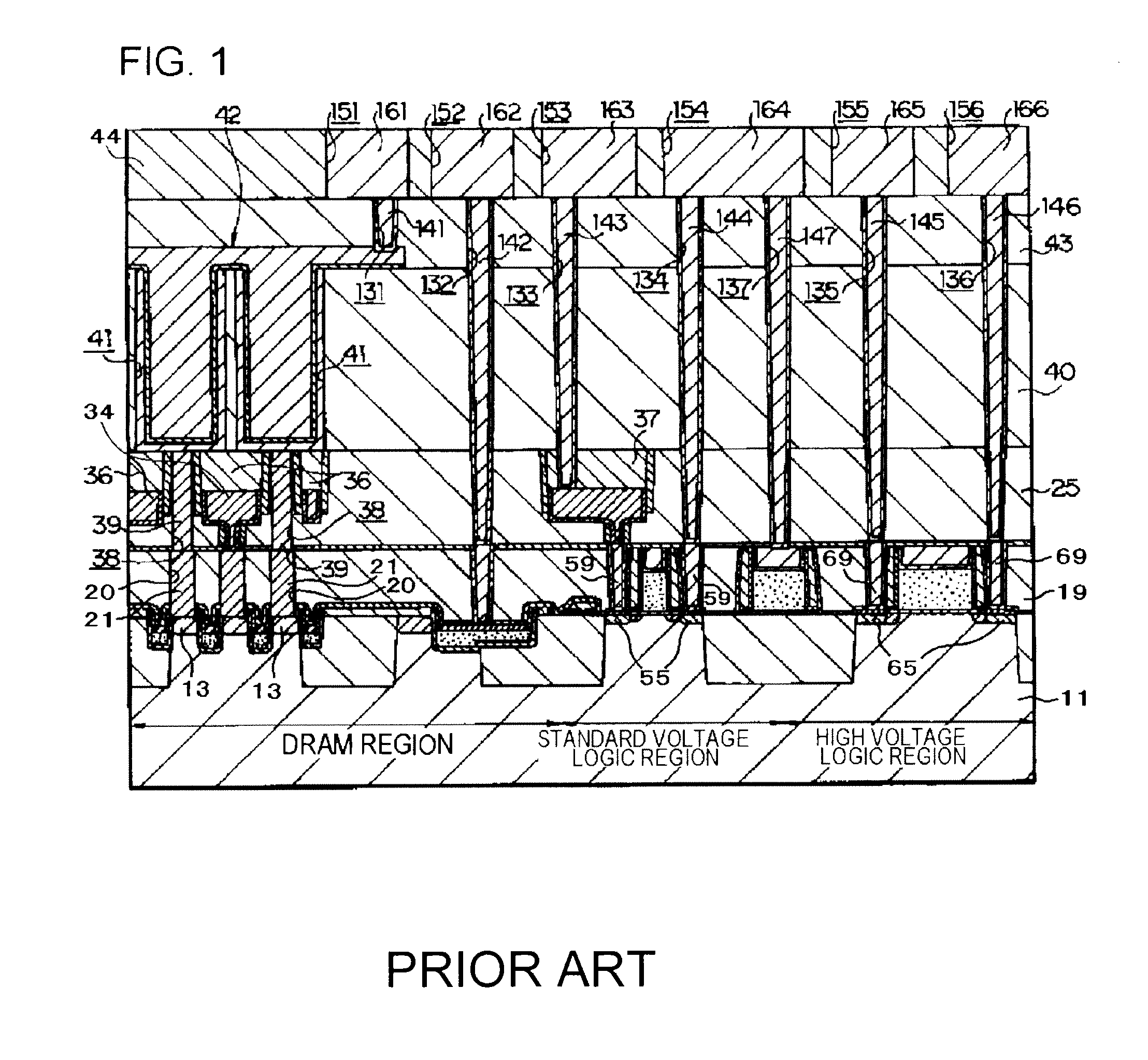
Since a cell area of a dynamic random access memory (DRAM) is smaller than a cell area of a static ram (SRAM), DRAM embedded logic LSIs have the advantage of being able to embed memory device of mass storage, and, on the other hand, they have a drawback that a DRAM forming process is required in addition to a process of forming the logic circuit, resulting in a high manufacturing cost.
For this reason, there is a problem that a groove having a high aspect ratio has to be formed with a high degree of accuracy, and a capacitor insulating film is required to be uniformly formed within the formed groove, which results in difficulty in thinning down.
Accordingly, there is another problem that the aspect ratio of the contact holes 134 to 136 is high, which causes an increase in the connection resistance.

Method used


Image

  • Memory embedded logic semiconductor device having memory region and logic circuit region
  • Memory embedded logic semiconductor device having memory region and logic circuit region
  • Memory embedded logic semiconductor device having memory region and logic circuit region

Examples


Embodiment Construction

[0034]The invention will be now described herein with reference to illustrative embodiments. Those skilled in the art will recognize that many alternative embodiments can be accomplished using the teachings of the present invention and that the invention is not limited to the embodiments illustrated for explanatory purposes.

[0035]Hereinafter, the embodiment of the invention will be described with reference to the accompanying drawings. In all the drawings, like elements are referenced by like reference numerals and descriptions thereof will not be repeated.

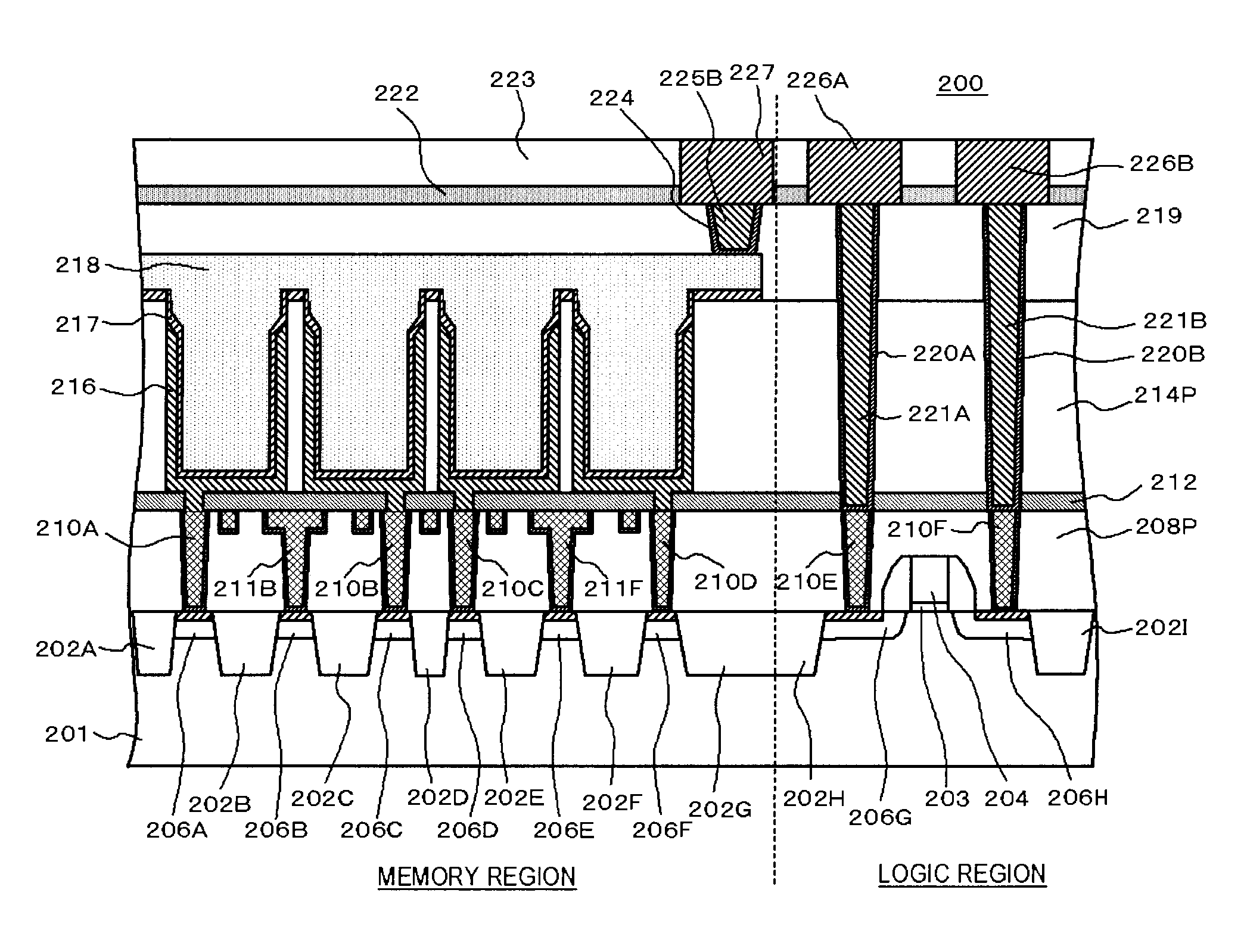
[0036]FIG. 2 is a cross-sectional view illustrating the schematic configuration of a semiconductor device 200 according to an embodiment of the invention. The semiconductor device 200 includes a cell transistor (not shown) formed in a memory region of a semiconductor substrate 201, and a logic device formed in a logic region of the semiconductor substrate 201. This logic device includes a logic transistor. In FIG. 2, the logic tra...


PUM


Abstract

In a method of manufacturing a semiconductor device, first contact holes reaching diffusion regions of a cell transistor, bit line contact holes reaching diffusion regions of the cell transistor, and interconnect grooves communicating with the bit line contact holes are buried in a first insulating film. In addition, first contact plugs and bit line contacts are respectively formed by burying conductive materials in the first contact holes, the bit line contact holes and the interconnect grooves, and the first contact plugs are electrically connected to a capacitor formed in a third insulating film through an opening formed in a second insulating film.

Description

[0001]The application is based on Japanese patent application No. 2009-194665, the content of which is incorporated hereinto by reference.BACKGROUND[0002]1. Technical Field[0003]The present invention relates to a memory embedded logic semiconductor device in which a memory section and a logic circuit are integrated on the same semiconductor substrate, and a method of manufacturing the same.[0004]2. Related Art[0005]In memory embedded logic LSIs, a memory section and a logic circuit are integrated on the same semiconductor substrate. Since a cell area of a dynamic random access memory (DRAM) is smaller than a cell area of a static ram (SRAM), DRAM embedded logic LSIs have the advantage of being able to embed memory device of mass storage, and, on the other hand, they have a drawback that a DRAM forming process is required in addition to a process of forming the logic circuit, resulting in a high manufacturing cost. As a structure of a memory cell of the DRAM, two types of structures,...

Claims


Application Information

Patent Timeline
Patent Type & Authority Patents(United States)
IPC IPC(8): H01L21/8238H01L21/8242
CPCH01L27/105H01L27/10894H01L27/10897H01L27/10814H10B12/315H10B12/50H10B12/09
Inventor AOKI, YASUYUKI
Owner RENESAS ELECTRONICS CORP
Learn More