Chip filter and the related supplementary tool
a chip filter and supplementary tool technology, applied in the direction of sustainable manufacturing/processing, coupling device connection, final product manufacturing, etc., can solve the problems of affecting the normal functioning of the local area network, wasting time and labor, and affecting the signal transmission, so as to reduce the material consumption of the connection terminal and facilitate the installation of the connection terminal. , the effect of quick and accurate bonding
- Summary
- Abstract
- Description
- Claims
- Application Information
AI Technical Summary
Benefits of technology
Problems solved by technology
Method used
Image
Examples
first embodiment
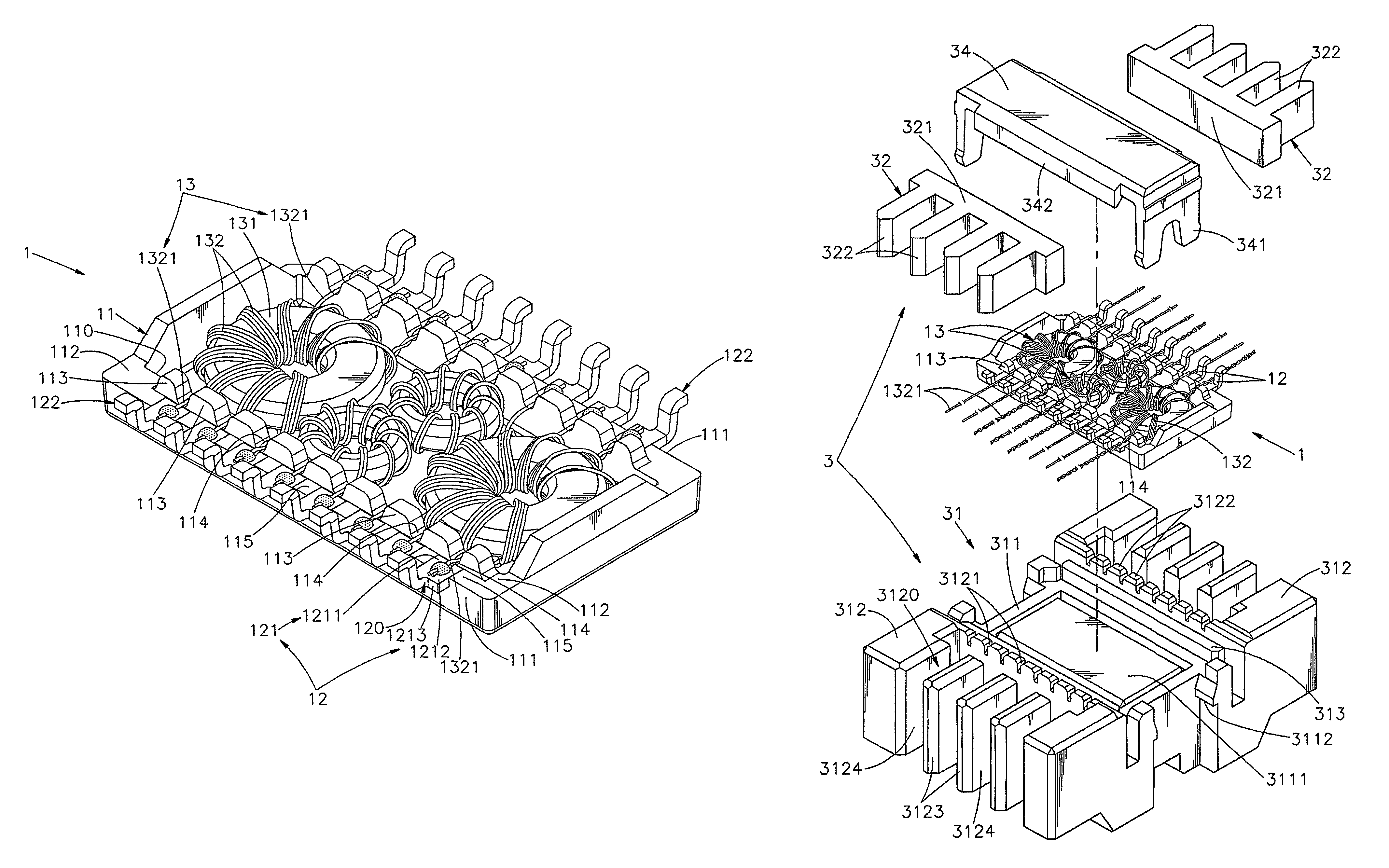
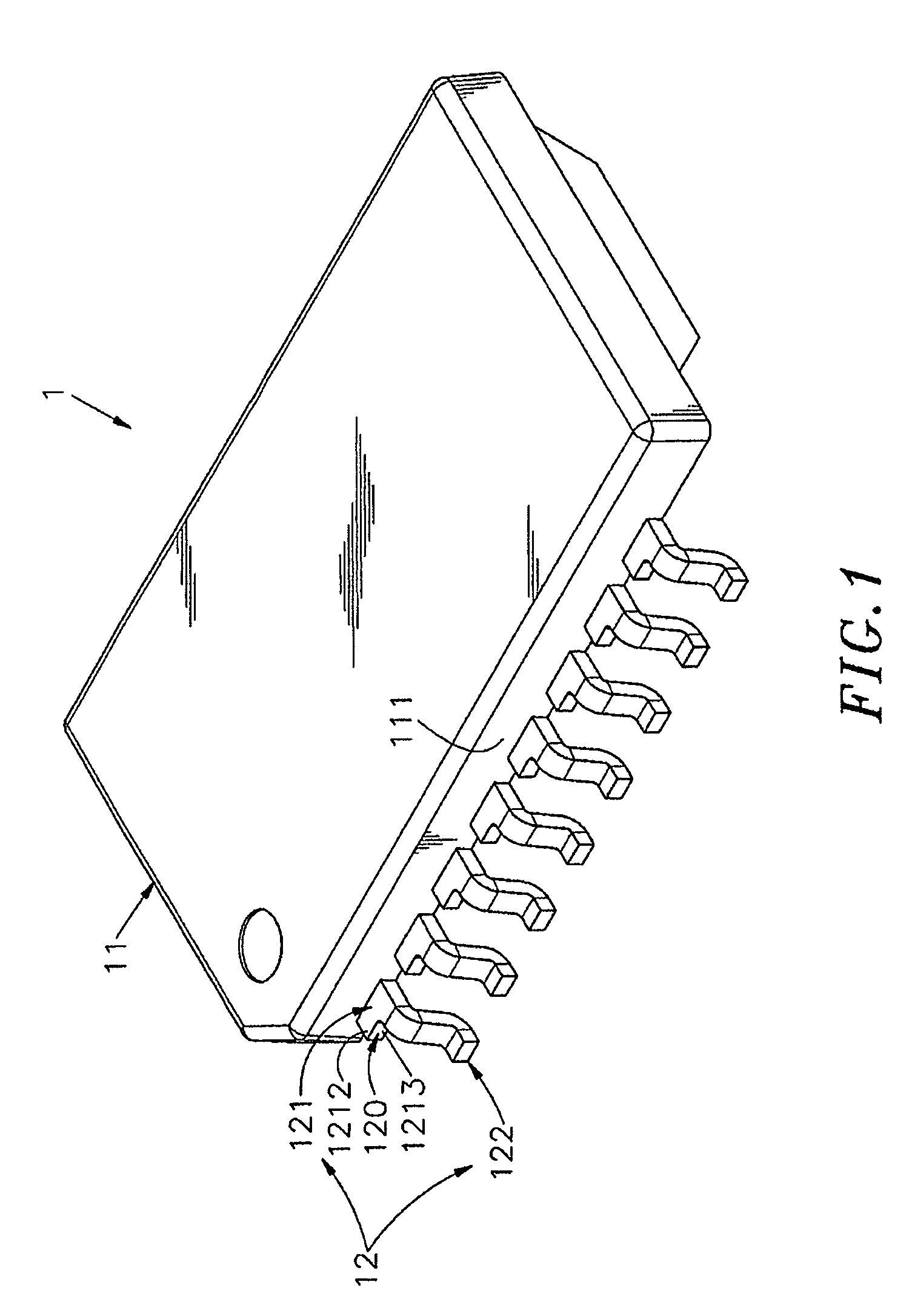
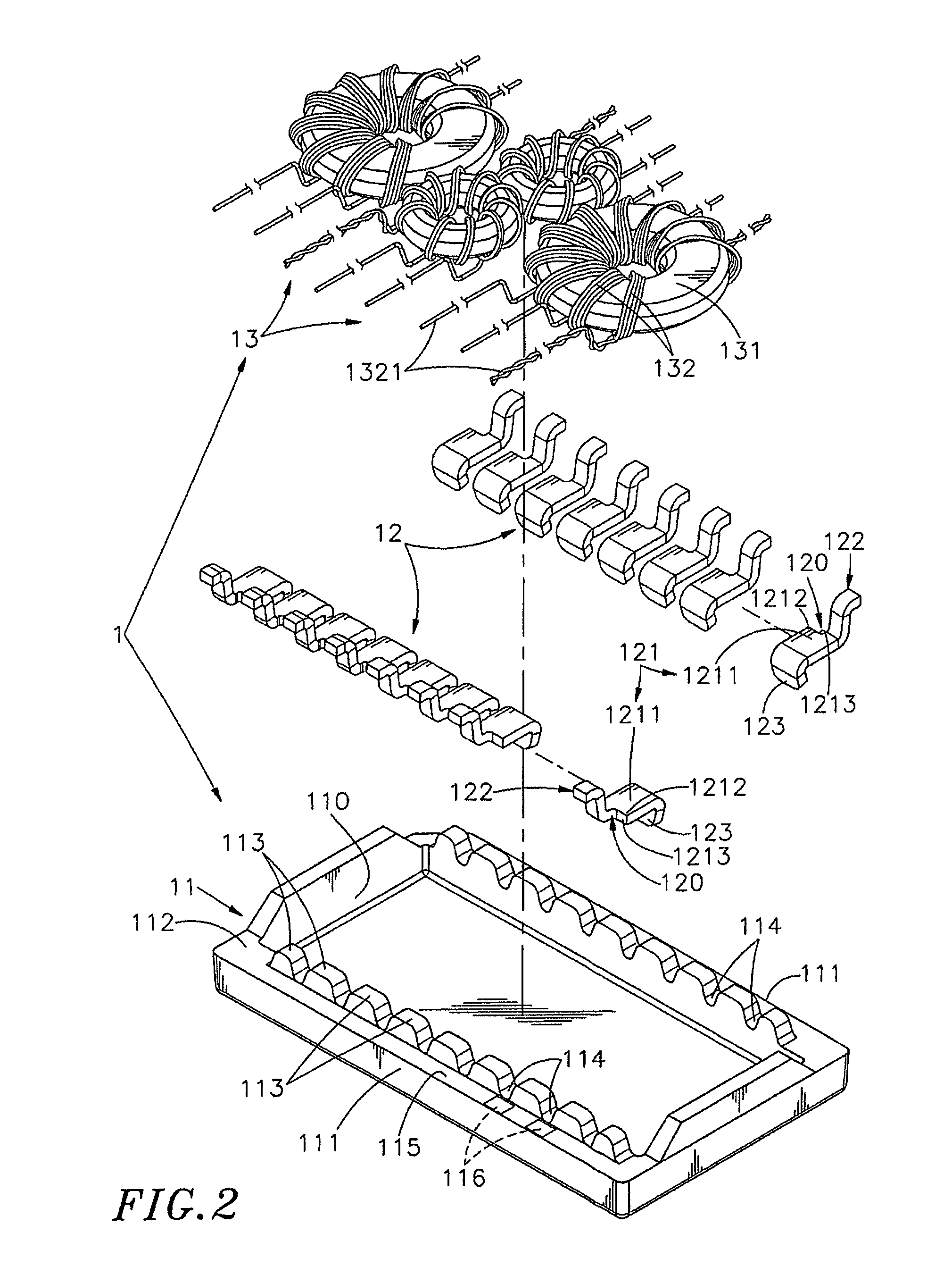
[0035]Referring to FIGS. 1˜4, a chip filter 1 in accordance with the present invention is shown comprising an insulative holder base 11, a plurality of connection terminals 12, and a plurality of filter elements 13.
[0036]The insulative holder base 11 has two opposing sidewalls 111, a recessed chamber 110 defined between the two sidewalls 111, two arrays of protruding blocks 113 respectively arranged along the sidewalls 111 adjacent to the recessed chamber 110 and protruding over the flat top edge 112 of each of the sidewalls 111, a wire groove 114 defined between each two adjacent protruding blocks 113 of each array of protruding blocks 113, a finished surface 115 formed on the flat top edge 112 of each of the sidewalls 111, and a plurality of soldering zones 116 defined in the finished surface 115 corresponding to the wire grooves 114.
[0037]The connection terminals 12 are bonded to the sidewalls 111 corresponding to the protruding blocks 113 during injection molding of the insulati...
second embodiment
[0042]FIGS. 6 and 7 illustrate a chip filter in accordance with the present invention. According to this alternate form, each connection terminal 12 comprises a base portion 121 bonded to one sidewall 111 corresponding to the location of one soldering zone 116 in the finished surface 115 of the associating sidewall 111, a soldering surface 1211 located on the base portion 121 and kept in flush with the top edge 112 of the associating sidewall 111, a bonding tip 122 extended from the base portion 121 out of the associating sidewall 111 for bonding to one respective surface contact 21 at an external circuit board 2 (see FIG. 7). The bonding tip 122 is generally inverted U-shaped having a vertical segment 1221 connected to the base portion 121 and embedded in the associating sidewall 111, a transverse segment 1222 extended from one end of the vertical segment 1221 remote from the base portion 121 to the outside of the associating sidewall 111, a supporting segment 1223 vertically downw...
PUM
 Abstract
Description
Claims
Application Information
 - R&D
- Intellectual Property
- Life Sciences
- Materials
- Tech Scout
- Unparalleled Data Quality
- Higher Quality Content
- 60% Fewer Hallucinations
Browse by: Latest US Patents, China's latest patents, Technical Efficacy Thesaurus, Application Domain, Technology Topic, Popular Technical Reports.
© 2025 PatSnap. All rights reserved.Legal|Privacy policy|Modern Slavery Act Transparency Statement|Sitemap|About US| Contact US: help@patsnap.com


