
Integrating design for reliability technology into integrated circuits

a reliability technology and integrated circuit technology, applied in reliability/availability analysis, power supply testing, instruments, etc., can solve the problems of significant variation in threshold voltage of non-nanoscale integrated circuit devices, power and robustness of digital ics, and significant spread of circuit delay, power and robustness for analog ics, and the growing complexity of system hardware defeats the enormous effort put forth by verification engineers to ensure system correctness

Inactive Publication Date: 2012-06-12
INT BUSINESS MASCH CORP
View PDF17 Cites 15 Cited by
  • Summary
  • Abstract
  • Description
  • Claims
  • Application Information

AI Technical Summary

Benefits of technology

This approach enables efficient design for reliability, reducing failure rates and costs by providing continuous monitoring and self-healing capabilities, improving the performance and longevity of semiconductor chips across their lifecycle.

Problems solved by technology

Nanoscale integrated circuit (IC) devices are prone to significant variation in threshold voltage caused by intrinsic aspects such as line-edge roughness, random dopant fluctuations, and body thickness variations in silicon-on-insulator devices.
Such variation can lead to significant spreads in circuit delay, power, and robustness for digital ICs, and performance for analogs ICs.
Furthermore, the growing complexity of system hardware is defeating the enormous effort put forth by verification engineers to ensure system correctness.
The reason is that verification is unable to keep up with modern high-productivity design solutions such as high-performance application specific integrated circuits (ASICs) and systems-on-a-chip (SoCs), which feature multiple complex hardware and software components connected by diverse sets of interfaces.
Today, most, if not all, complex system designs are released containing latent bugs, which sometimes become evident only after a design reaches the market.
Ultimately, these challenges threaten the continued scaling of silicon fabrication technologies.
As devices scale to smaller geometries, however, they become less reliable, necessitating the inclusion of design for reliability features.
These costs are increasing at technology nodes with higher natural failure rates, which require more robust and finer-grained reliability techniques.

Method used


Image

  • Integrating design for reliability technology into integrated circuits
  • Integrating design for reliability technology into integrated circuits
  • Integrating design for reliability technology into integrated circuits

Examples


Embodiment Construction

[0021]The embodiments of the invention and the various features and advantageous details thereof are explained more fully with reference to the non-limiting embodiments that are illustrated in the accompanying drawings and detailed in the following description. It should be noted that the features illustrated in the drawings are not necessarily drawn to scale. Descriptions of well-known components and processing techniques are omitted so as to not unnecessarily obscure the embodiments of the invention. The examples used herein are intended merely to facilitate an understanding of ways in which the embodiments of the invention may be practiced and to further enable those of skill in the art to practice the embodiments of the invention. Accordingly, the examples should not be construed as limiting the scope of the embodiments of the invention.

[0022]For a given application condition, there is a growing gap between the expected reliability targets of semiconductor products and the speci...


PUM


Abstract

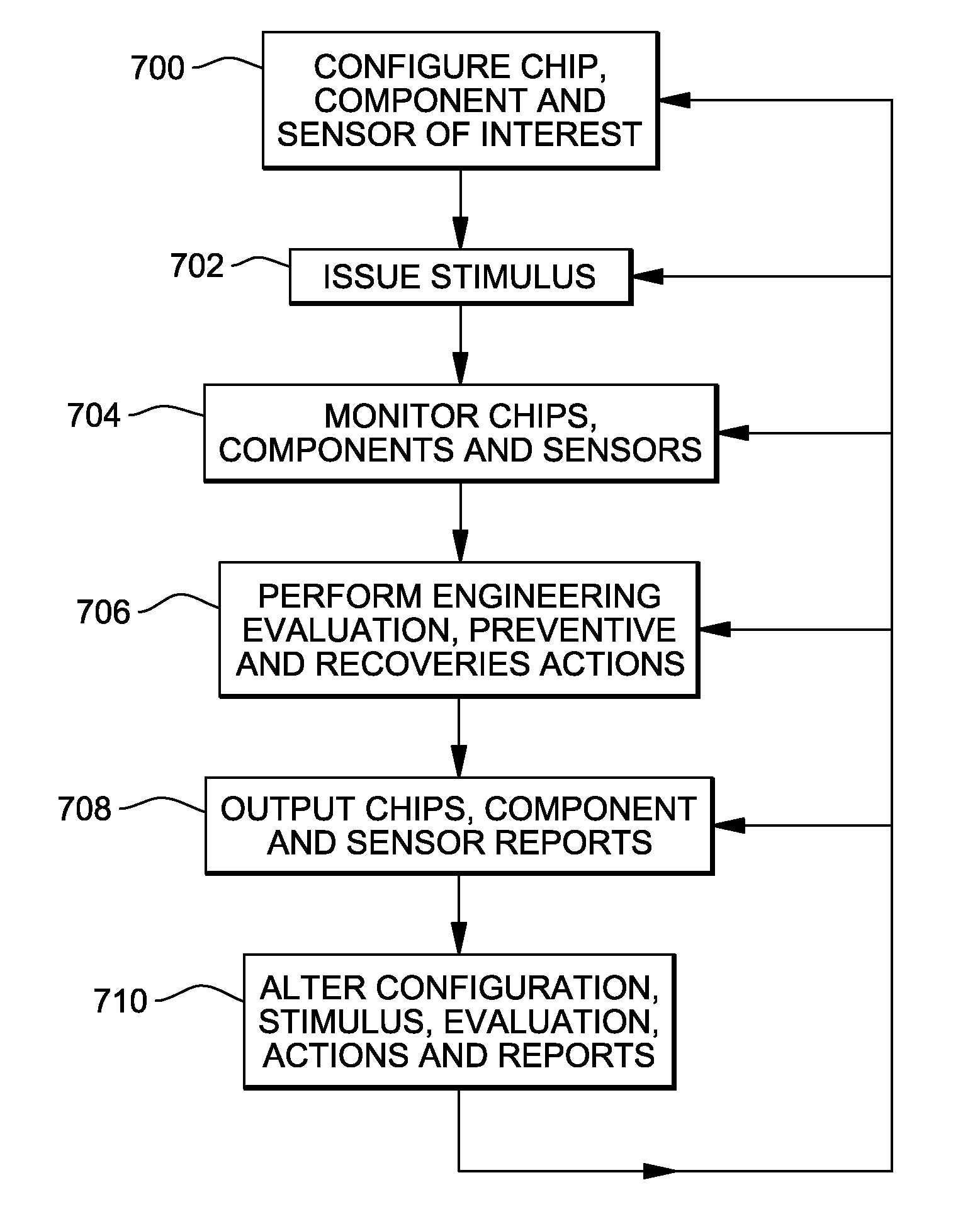
A method executes computerized instructions within an integrated and packaged semiconductor device using a centralized programming interface within the packaged semiconductor device to perform in-system preventive and recovery actions, configure and issue stimulus to chips, components and sensors within the semiconductor device. The method monitors chip, components and sensors within the packaged semiconductor device, using the centralized programming interface, to measure characteristics of the packaged semiconductor device in response to the stimulus. The structure including chips, components and sensors produce outputs representing the characteristics. The method performs an evaluation to determine whether the chip, component and sensor outputs are within predetermined limits, using the centralized programming interface; and reports occurrences of instances of the chip, component and sensor outputs being outside the predetermined limits, using the centralized programming interface, to an on-chip storage medium, external test equipment or computerized device outside of the packaged semiconductor device.

Description

BACKGROUND OF THE INVENTION[0001]1. Field of the Invention[0002]The embodiments herein generally relate to integrated circuit chips and more particularly to an integrated circuit chip having an enhanced programming and test interface and an associated method of monitoring, healing and testing the chip using the enhanced programming and test interface.[0003]2. Description of Related Art[0004]Nanoscale integrated circuit (IC) devices are prone to significant variation in threshold voltage caused by intrinsic aspects such as line-edge roughness, random dopant fluctuations, and body thickness variations in silicon-on-insulator devices. Such variation can lead to significant spreads in circuit delay, power, and robustness for digital ICs, and performance for analogs ICs.[0005]Furthermore, the growing complexity of system hardware is defeating the enormous effort put forth by verification engineers to ensure system correctness. The reason is that verification is unable to keep up with mod...

Claims


Application Information

Patent Timeline
Patent Type & Authority Patents(United States)
IPC IPC(8): G01R31/3173G01R31/40
CPCG06F11/008G06F2201/81G06F2201/86
Inventor GRAAS, CAROLE D.NSAME, PASCAL A.
Owner INT BUSINESS MASCH CORP
Learn More