
Dicing die-bonding film

a die-bonding film and die-bonding technology, applied in the direction of film/foil adhesives, adhesive types, transportation and packaging, etc., can solve the problems of excessive anchoring effect, difficult peeling, and bonding film, and achieve excellent pickup properties, easy peeling, and preventing chip fly

Inactive Publication Date: 2012-02-21
NITTO DENKO CORP
View PDF14 Cites 8 Cited by
  • Summary
  • Abstract
  • Description
  • Claims
  • Application Information

AI Technical Summary

Benefits of technology

The solution provides improved peeling properties and prevents chip fly and adhesive residue, enabling efficient pickup of semiconductor chips without warping or reattachment of cut faces, enhancing the yield and reliability of semiconductor device manufacturing.

Problems solved by technology

When a dicing die-bonding film that is produced by laminating the die-bonding film onto the pressure-sensitive adhesive layer before the ultraviolet ray irradiation is used, the adhesion at the interface of the pressure-sensitive adhesive layer and the die-bonding film is high and the anchor effect is excessively expressed; as a result, they found that there is a case where peeling becomes difficult even when the pressure-sensitive adhesive layer is cured by ultraviolet ray irradiation and the semiconductor chip is picked up.
As a result, warping may occur over the entire dicing die-bonding film.

Method used

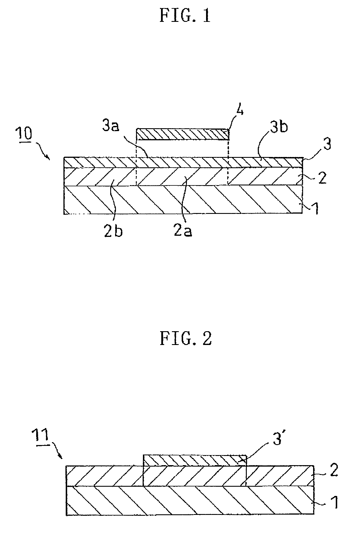
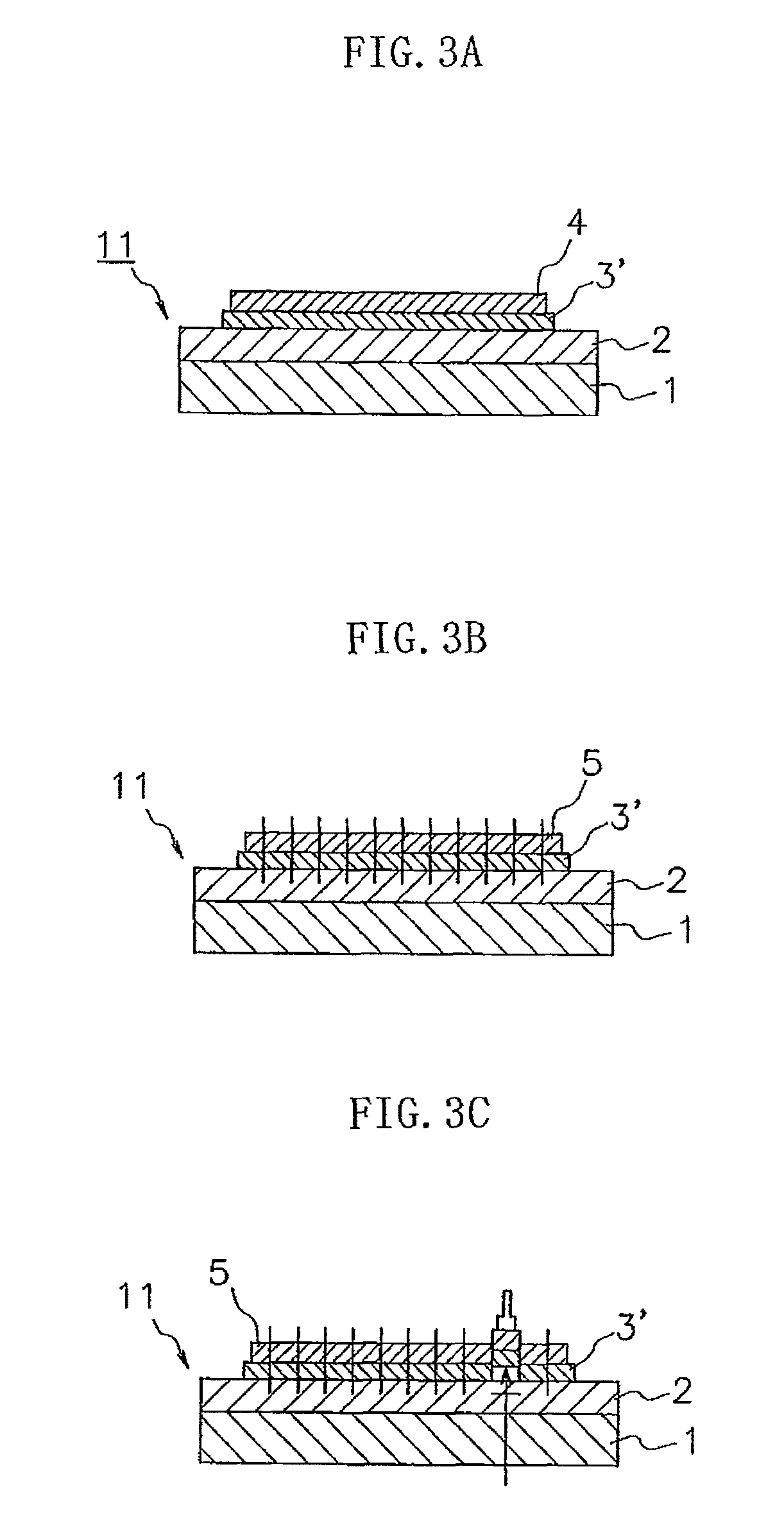
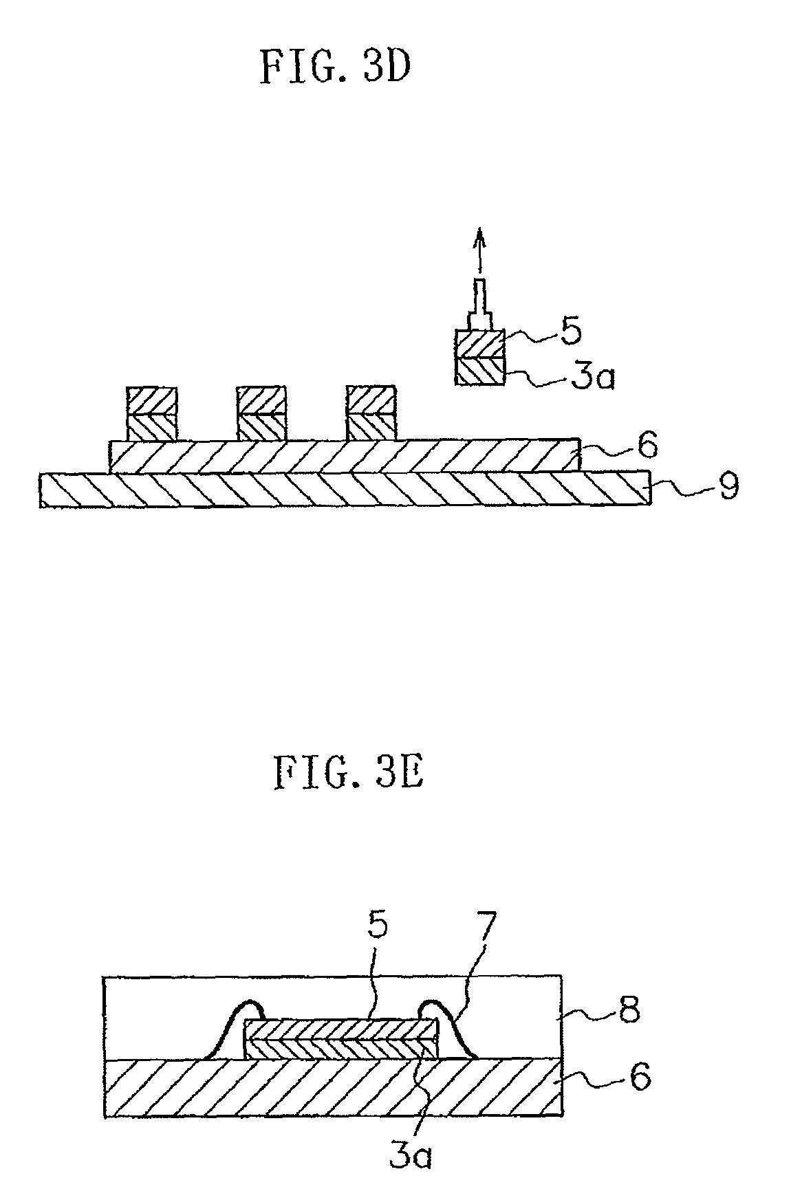

Image

  • Dicing die-bonding film
  • Dicing die-bonding film
  • Dicing die-bonding film

Examples


example 1

[0105]

[0106]Acrylic polymer A having a weight average molecular weight of 580,000 was obtained by placing 51.7 parts of 2-ethylhexyl acrylate (hereinafter referred to as “2EHA”), 39.0 parts of stearyl acrylate (hereinafter referred to as “SA”), 9.3 parts of 2-hydroxyethyl acrylate (below, referred to as “HEA”), 0.2 parts of benzoyl peroxide, and 65 parts of toluene into a reactor equipped with a cooling tube, a nitrogen-introducing tube, a thermometer, and a stirring apparatus, and performing a polymerization treatment at 61° C. in a nitrogen airflow for 6 hours. The weight average molecular weight is as follows. The molar ratio of 2EHA to SA to HEA was made to be 70 mol:30 mol:20 mol.

[0107]An acrylic polymer A′ was obtained by adding 10.0 parts (80 mol % to HEA) of 2-methacryloyloxyethyl isocyanate (in the following, referred to as “MOI”) into this acrylic polymer A and performing an addition reaction treatment at 50° C. in an air flow for 48 hours.

[0108]Next, a pressure-sensitive ...

examples 2 to 13

[0129]In each of Examples 2 to 13, the dicing die-bonding film was produced in the same manner as in Example 1 except that the composition and the compounded ratio were changed to those shown in Table 1.

[0130]

TABLE 1HYDROXYLGROUP-ACRYLICACRYLICCONTAININGISOCYANATEESTER AESTER BMONOMERCOMPOUNDPHOTOPOLYMERIZATION2EHAi-OASAVABAHEA4HBAMOIAOITOLUENEC / LINITIATOREXAMPLE 151.7—39.0—— 9.3—10.06585(70)  (30)  (20)  (80)  EXAMPLE 253.7—40.5—— 5.8— 6.4—6585(70)  (30)  (12)  (83)  EXAMPLE 349.4—37.3——13.3—14.3—6585(70)  (30)  (30)  (80)  EXAMPLE 468.5—44.3——10.2—10.9—6585(85)  (35)  (20)  (80)  EXAMPLE 546.7—39.0—— 9.1— 9.7—6585(65)  (30)  (20)  (80)  EXAMPLE 6—51.738.2—— 9.3—10.0—6585(70)  (30)  (20)  (80)  EXAMPLE 750.6—38.2———11.3 9.7—6585(70)  (30)  (20)  (80)  EXAMPLE 851.7—39.0—— 9.3——  9.16585(70)  (30)  (20)  (80)EXAMPLE 951.7—39.0—— 9.3— 8.7—6585(70)  (30)  (20)  (70)  EXAMPLE51.7—39.0—— 9.3—11.2—658510(70)  (30)  (20)  (90)  EXAMPLE51.7—39.0—— 9.3—10.0—1008511(70)  (30)  (20)  (80)  EX...


PUM

PropertyMeasurementUnit
thicknessaaaaaaaaaa
thicknessaaaaaaaaaa
thicknessaaaaaaaaaa

Abstract

A dicing die-bonding film having a pressure-sensitive adhesive layer on a base and a die-bonding film on the pressure-sensitive adhesive layer, the pressure-sensitive adhesive layer comprising an acrylic polymer comprising acrylic ester A represented by CH2═CHCOOR1 (where R1 is an alkyl group having 6-10 carbon atoms), acrylic ester B represented by CH2═CHCOOR2 (where R2 is an alkyl group having 11 carbon atoms or more), a hydroxyl group-containing monomer, and an isocyanate compound having a radical reactive carbon-carbon double bond where the ratios of components are 40-10 mol % of the acrylic ester B with respect to 60-90 mol % of the acrylic ester A, 10-30 mol % hydroxyl group-containing monomer with respect to 100 mol % of the total of the acrylic ester A and the acrylic ester B, and 70-90 mol % isocyanate compound with respect to 100 mol % of the monomer containing a hydroxl group.

Description

[0001]This application claims priority to Japanese Patent Application No. 2008-200983, filed Aug. 4, 2008. The above-referenced application is hereby expressly incorporated by reference in its entirety.BACKGROUND OF THE INVENTION[0002]1. Field of the Invention[0003]The present invention relates to a dicing die-bonding film that is used in dicing of a workpiece under a condition where an adhesive for fixing a chip-shaped workpiece such as a semiconductor chip and an electrode member is pasted onto a workpiece such as a semiconductor wafer before dicing, a manufacturing method thereof, and a method of manufacturing a semiconductor device using it.[0004]2. Description of the Related Art[0005]A semiconductor wafer (workpiece) on which a circuit pattern is formed is diced into semiconductor chips (chip-shaped workpieces) (a dicing step) after the thickness thereof is adjusted by backside polishing as necessary. In the dicing step, it is common to wash the semiconductor wafer at an approp...

Claims


Application Information

Patent Timeline
Patent Type & Authority Patents(United States)
IPC IPC(8): B32B7/12B32B15/04C09J7/22C09J7/30
CPCC08F220/18C09J7/0239C09J133/08C09J163/00H01L21/6836H01L24/27H01L24/83H01L24/29C08F220/34C08F2220/1808C08F2220/1833C08F2220/281C09J2201/36C09J2201/606C09J2203/326C09J2205/31C09J2433/00C09J2463/00H01L24/85H01L2221/68327H01L2224/2919H01L2224/48227H01L2224/83191H01L2224/83855H01L2224/92H01L2224/92247H01L2924/01005H01L2924/01013H01L2924/01015H01L2924/01016H01L2924/01025H01L2924/01027H01L2924/01029H01L2924/01033H01L2924/01047H01L2924/01051H01L2924/01056H01L2924/01074H01L2924/01075H01L2924/01079H01L2924/01082H01L2924/07802H01L2924/19042H01L2924/3025H01L2224/32225H01L2224/73265H01L2924/01006H01L2924/01019H01L2924/014H01L2924/0665H01L2224/85H01L2224/32245H01L2224/48247H01L2924/15747Y10T428/2848Y10T428/2891Y10T428/28H01L2924/00H01L2924/00012H01L2924/15788H01L2924/181H01L2224/48091H01L24/73H01L2924/00014H01L24/48C09J7/22C09J7/30Y10T428/31511C08F220/281C09J2301/208C09J2301/416C09J2301/302C08F220/1808H01L2224/45015H01L2924/207H01L2224/45099C09J175/00H01L21/30H01L21/78
Inventor KAMIYA, KATSUHIKOMATSUMURA, TAKESHIMURATA, SHUUHEIOOTAKE, HIRONAO
Owner NITTO DENKO CORP
Learn More