AlxInyGa1-x-yN mixture crystal substrate, method of growing same and method of producing same

a technology of mixture crystal substrate and alxinyga1, which is applied in the direction of crystal growth process, polycrystalline material growth, chemically reactive gas growth process, etc., can solve the problems of many defects in the aln film, and achieve the effect of absorbing material gasses higher and efficiently

Inactive Publication Date: 2011-11-29
SUMITOMO ELECTRIC IND LTD
View PDF31 Cites 1 Cited by
  • Summary
  • Abstract
  • Description
  • Claims
  • Application Information

AI Technical Summary

Benefits of technology

[0027]This invention produces low dislocation density AlxInyGa1-x-yN mixture crystal substrate by preparing an undersubstrate, forming regularly allotted dotted masks on the undersubstrate, growing AlxInyGa1-x-yN mixture crystal, forming facet pits and closed defect accumulating regions above the dotted masks, attracting dislocations via the facets into the defect accumulating regions, arresting the dislocations in the defect accumulating regions (H) and reducing dislocation density in other regions except the defect accumulating regions (H). The present invention succeeds in making the best use of the seeds pre-formed on a substrate, the closed defect accumulating regions (H) followed by the seeds and the facet growth induced by the seeds. The facet growth minimizes dislocation density of the regions in growing AlxInyGa1-x-yN crystal except the closed defect accumulating regions (H) by sweeping many dislocations into the bottoms of facet pits. The closed defect accumulating regions (H) hold many dislocations captive. The seed-defined closed defect accumulating regions (H) and the facet growth enable us to make low dislocation density AlxInyGa1-x-yN mixture crystals.
[0029]The present invention succeeds in producing a low-dislocation AlxInyGa1-x-yN mixture crystal substrate by controlling the positions of the closed defect accumulating regions (H) which gather the dislocations from other regions by implanting seeds on a starting substrate in accordance with designed patterns having some regularity. The AlxInyGa1-x-yN substrate crystal made by the present invention is a low-dislocation single crystal in Z and Y except the definite small regions (closed defect accumulating regions (H)). The present invention can supply low-defect density AlxInyGa1-x-yN mixture crystal substrates. AlxInyGa1-x-yN mixture crystal substrate wafers are best for making light emitting diodes (LEDs) or laser diodes (LDs) having wavelengths between 200 nm and 1300 nm.
[0033]The MOC method employs Al-, In- Ga-including metallorganic compounds (e.g., trimethylaluminum, trimethylindium, trimethylgallium) as Al, In, Ga materials like the MOCVD. The nitrogen material is ammonia (NH3) gas. Unlike the MOCVD, TMA, TMI and TMG do not react with ammonia (NH3). In a hot wall type furnace, TMA, TMI and TMG react with HCl gas for synthesizing AlCl3, InCl, GaCl. Vapors AlCl3, InCl and GaCl fall toward a heated substrate on a susceptor. The substrate is supplied with ammonia gas. AlCl3, InCl and GaCl react with ammonia for making AlInGaN. AlxInyGa1-x-yN piles upon the substrate and makes a thick AlxInyGa1-x-yN film. The use of the metallorganic compounds s(TMA, TMI, TMG) may induce contamination by carbon. However, this method can absorb material gasses higher efficiently than the MOCVD method.

Problems solved by technology

If aluminum nitride AlN films were grown on an obtainable GaN substrate, the AlN film would be plagued with many defects.

Method used


Image

  • AlxInyGa1-x-yN mixture crystal substrate, method of growing same and method of producing same
  • AlxInyGa1-x-yN mixture crystal substrate, method of growing same and method of producing same
  • AlxInyGa1-x-yN mixture crystal substrate, method of growing same and method of producing same

Examples


embodiment 1

Al0.8Ga0.2N Made on Sapphire Undersubstrate, Samples A, B, C and D; FIG. 11

[0243]FIG. 11 shows steps of making an Al0.8Ga0.2N substrate as Embodiment 1. A starting undersubstrate is a sapphire C-plane wafer 51. FIG. 11(1) denotes the sapphire undersubstrate 51. Sapphire has trigonal symmetry. Al0.8Ga0.2N has hexagonal symmetry. A “substrate” is different from an “undersubstrate”, here. Don't confuse a “substrate” with an “undersubstrate”. The undersubstrate is a starting plate. The substrate is a final product.

[0244]A 2 μm thick Al0.8Ga0.2N epi-layer 52 is preliminarily made on the sapphire undersubstrate 51 by an MOCVD method. Samples have an Al0.8Ga0.2N C-plane surface.

[0245]A 100 nm thick SiO2 film is formed upon the Al0.8Ga0.2N epi-layer 52 for distributing many seeds regularly and making a seed pattern on the epi-layer 52. The seed pattern 53 is a hexagonal pattern having many round dots 53 placed at corner points of equivalent equilateral triangles having a side aligning in t...

embodiment 2

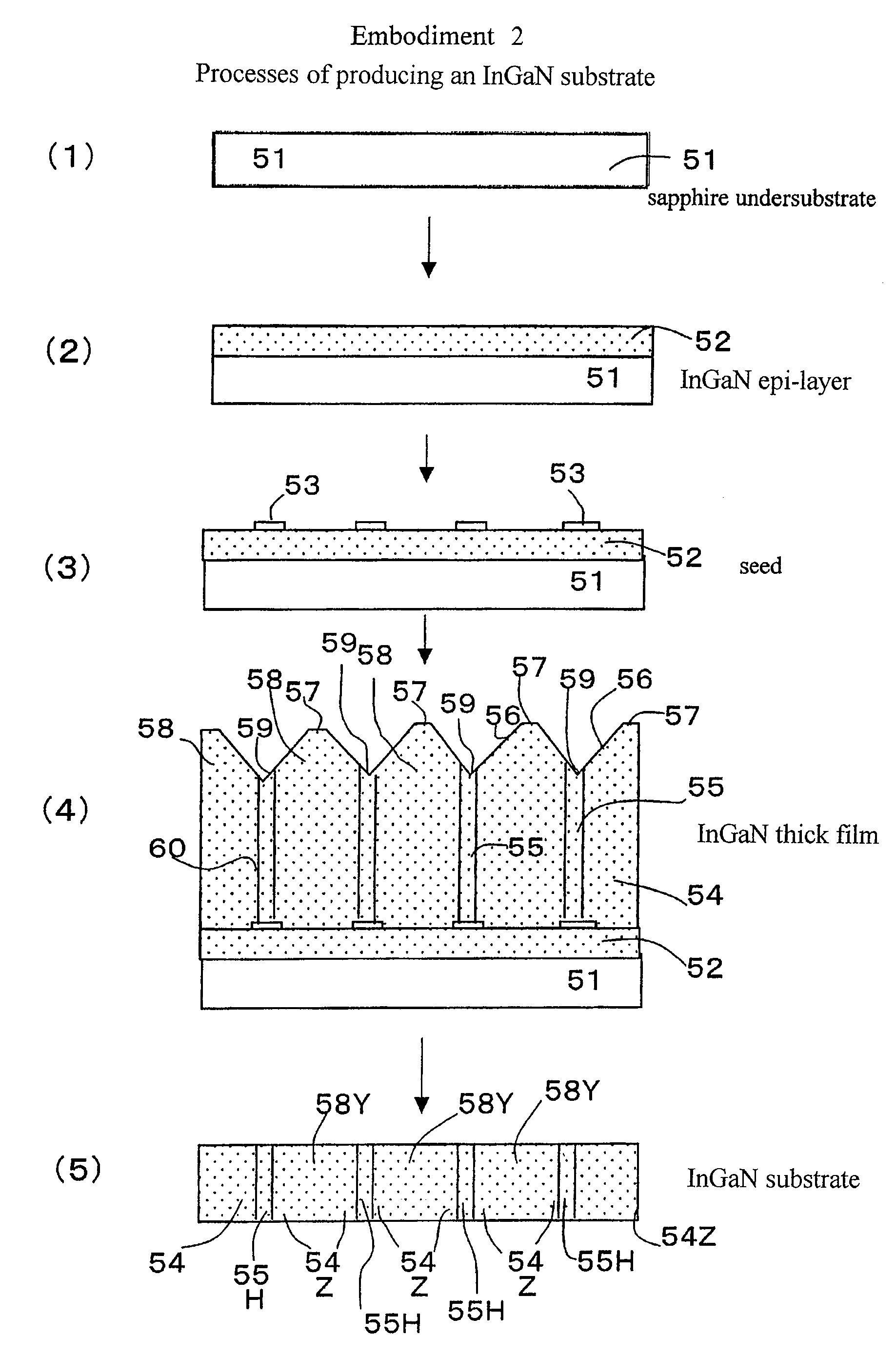
In0.9Ga0.1N on Sapphire Undersubstrate, FIG. 12

[0309]FIG. 12 shows steps of making an In0.8Ga0.1N substrate as Embodiment 2. A starting undersubstrate is a sapphire C-plane wafer 51. FIG. 12(1) denotes the sapphire undersubstrate 51. Sapphire has trigonal symmetry. In0.9Ga0.1N has hexagonal symmetry.

[0310]A 2 μm thick In0.9Ga0.1N epi-layer 52 is preliminarily made on the sapphire undersubstrate 51 by an MOCVD method. Samples have an In0.9Ga0.1N C-plane surface.

[0311]A 100 nm thick SiO2 film is formed upon the In0.9Ga0.1N epi-layer 52 for distributing many seeds regularly and making a seed pattern on the epi-layer 52. The seed pattern 53 is a hexagonal pattern having many round dots 53 placed at corner points of equivalent equilateral triangles having a side aligning in two dimensional directions without extra margin on the epi-layer. Seeds of SiO2 in the predetermined pattern are formed by etching other parts of round dots allotted on the corner points of the basic triangles by pho...

embodiment 3

Al0.3Ga0.3In0.4N: on GaAs, Si, Sapphire Substrate; Pattern A, H(=A+ELO); Samples J, K, L, M; FIG. 13

[0375]Embodiment 3 prepared three kinds of foreign material undersubstrates for making Al0.3Ga0.3In0.4N substrate crystals.

[0376]α. (111) GaAs undersubstrate

[0377]β. C-plane (0001) sapphire undersubstrate

[0378]γ. (111) Si undersubstrate

[0379]Silicon (Si) has the diamond structure of cubic symmetry group. Gallium arsenide (GaAs) has the zinc blende structure of cubic symmetry group. Al0.3Ga0.3In0.4N has hexagonal symmetry. In cubic symmetry crystals, only a (111) plane has three-fold rotation symmetry. Thus, a (111) plane is employed for Si and GaAs. Sapphire has trigonal symmetry which lacks three-fold rotation symmetry. Thought the c-axis does not have three-fold rotation symmetry, a (0001)C-plane sapphire can be utilized as an undersubstrate of Al0.3Ga0.3In0.4N growth.

[0380]FIG. 12(1), (2) and (3) show steps of the Al0.3Ga0.3In0.4N growth. Unlike Embodiments 1 and 2 Samples A to D, ...


PUM

PropertyMeasurementUnit
diametersaaaaaaaaaa
diameteraaaaaaaaaa
absorption light wavelengthaaaaaaaaaa

Abstract

Seeds are implanted in a regular pattern upon an undersubstrate. An AlxInyGa1-x-yN (0≦x≦1, 0≦y≦1, 0<x+y≦1) mixture crystal is grown on the seed implanted undersubstrate by a facet growth method. The facet growth makes facet pits above the seeds. The facets assemble dislocations to the pit bottoms from neighboring regions and make closed defect accumulating regions (H) under the facet bottoms. The closed defect accumulating regions (H) arrest dislocations permanently. Release of dislocations, radial planar defect assemblies and linear defect assemblies are forbidden. The surrounding accompanying low dislocation single crystal regions (Z) and extra low dislocation single crystal regions (Y) are low dislocation density single crystals.

Description

RELATED APPLICATIONS[0001]This application is a divisional of U.S. patent application Ser. No. 11 / 501,817, filed Aug. 10, 2006 now U.S. Pat. No. 7,655,960, which is a divisional of U.S. patent application Ser. No. 11 / 041,202, filed Jan. 25, 2005, now U.S. Pat. No. 7,105,865, which is a continuation-in-part of U.S. patent application Ser. No. 10 / 700,495, filed Nov. 5, 2003, now U.S. Pat. No. 7,112,826, which is a divisional of U.S. patent application Ser. No. 10 / 246,559, filed Sep. 19, 2002, now U.S. Pat. No. 6,667,184, which claims priority of Japanese Patent application Nos. 2001-284323, filed Sep. 19, 2001 and 2002-230925, filed Aug. 8, 2002, the contents of which are herewith incorporated by reference.BACKGROUND OF THE INVENTION[0002]1. Field of the Invention[0003]This invention relates to an aluminum indium gallium nitride (AlxInyGa1-x-yN: 0≦x≦1, 0≦y≦1, 0<x+y≦1) mixture crystal substrate for producing ultraviolet, blue light emitting diodes (LEDs) and ultraviolet, blue light ...

Claims


Application Information

Patent Timeline
Patent Type & Authority Patents(United States)
IPC IPC(8): H01L21/20C30B25/02C30B25/18C30B29/40
CPCC30B25/02H01L21/02647C30B25/183C30B29/40C30B29/403C30B29/406H01L21/02381H01L21/02395H01L21/0242H01L21/02433H01L21/02458H01L21/0254H01L21/02609H01L21/02642C30B25/18
Inventor NAKAHATA, SEIJIHIROTA, RYUMOTOKI, KENSAKUOKAHISA, TAKUJIUEMATSU, KOUJI
Owner SUMITOMO ELECTRIC IND LTD
Why Eureka
Try Eureka