
Method for fabricating CuInS2 thin film by metal organic chemical vapor deposition, CuInS2 thin film fabricated by the same and method for fabricating In2S3 thin film therefrom

a technology of metal organic chemical vapor deposition and cuins2 thin film, which is applied in the direction of chemical vapor deposition coating, coating, semiconductor devices, etc., can solve the problems of limited reduction of material costs, complex chemical structure and commercially successful technology of thin film solar cells has not yet been developed

Inactive Publication Date: 2011-11-08
SAMSUNG SDI CO LTD +2
View PDF18 Cites 3 Cited by
  • Summary
  • Abstract
  • Description
  • Claims
  • Application Information

AI Technical Summary

Benefits of technology

This approach enables the production of high-purity CuInS2 thin films with a tetragonal structure and a band gap of 1.4 to 1.6 eV, suitable for solar cells, while reducing fabrication costs and simplifying the process by allowing for controlled deposition conditions and the use of MOCVD under both argon and vacuum atmospheres.

Problems solved by technology

Although crystalline silicon solar cells have a possibility for cost reduction by means of mass-production, they utilize bulky silicon as a raw material, thus having a limitation in reducing material costs.
Despite such circumstances, thin film solar cells have a complicated chemical structure and necessarily involve deposition of several micrometers of a plurality of ultra-thin films.
For these reasons, a commercially successful technology for thin film solar cells has not yet been developed.
Both the physical and chemical methods require complicated process conditions of low vapor pressure and constant solution concentration ratio to fabricate chalcogenide thin films having a specific composition.
In addition, these methods have advantages of relatively low fabrication costs and simple fabrication equipment, but disadvantageously make it difficult to adjust a composition of chalcogenide to a desired level due to inherent characteristics thereof and to secure reproducibility in the thickness and uniformity of thin films.
Vacuum evaporation involves a complicated and troublesome procedure to deposit chalcogen elements with a desired composition due to different volatilities.
In addition, vacuum evaporation has a problem of the necessity of the supplement of elements lost from deposition and subsequent thermal processing at a high temperature for phase formation [U.S. Pat. No. 6,323,417].
The chemical bath deposition has general problems associated with wet processes and its application is limited to CdS thin films.
However, these organometallic single precursors have problems in that various metals are particularly restricted in their use to fabricate chacogenide thin films involving the necessity of various components and compositions, and an insufficient content of highly volatile sulfur (S) or selenium (Se) is used in preparation of chalcogenide composed of multimetals, as similar to vacuum evaporation.

Method used


Image

  • Method for fabricating CuInS2 thin film by metal organic chemical vapor deposition, CuInS2 thin film fabricated by the same and method for fabricating In2S3 thin film therefrom
  • Method for fabricating CuInS2 thin film by metal organic chemical vapor deposition, CuInS2 thin film fabricated by the same and method for fabricating In2S3 thin film therefrom
  • Method for fabricating CuInS2 thin film by metal organic chemical vapor deposition, CuInS2 thin film fabricated by the same and method for fabricating In2S3 thin film therefrom

Examples


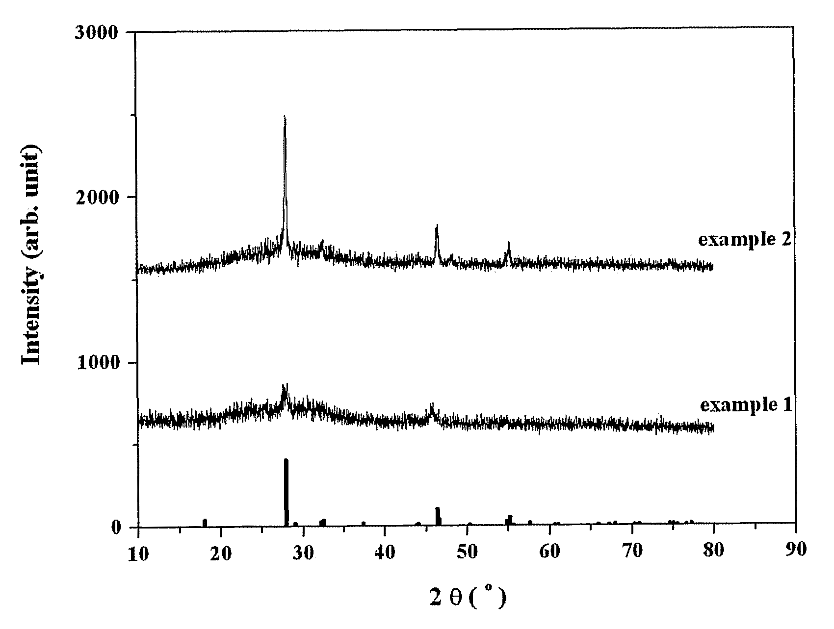
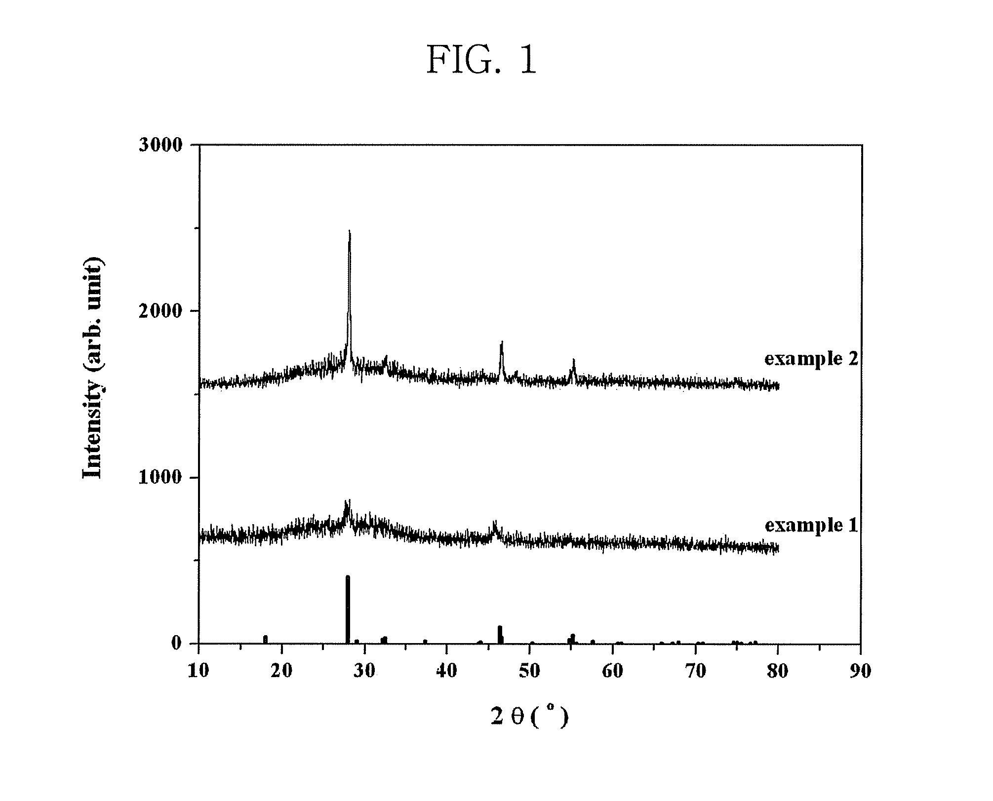
example 1

Fabrication of CuInS2 Thin Film (A-CIS-1) Under Argon Atmosphere

[0073]Step 1: Fabrication of Copper Thin Film Under Argon Atmosphere

[0074]The copper ethylbutyrylacetate precursor prepared in Preparative Example 1 was recrystallized using a common technique. A washed clean substrate was fixed in deposition equipment. Prior to the deposition, the inside of a reactor was repeatedly cleaned with argon (Ar) as a carrier gas, and was stood under vacuum for one hour or more. As a result, residues such as oxygen and water, which are in danger of being incorporated in a thin film and becoming impurities therein, were removed from the inwalls of the reactor. Then, the copper ethylbutyrylacetate precursor was put in an evaporator equipped with a bubbler. The copper ethylbutyrylacetate precursor was deposited on a glass substrate under an argon (Ar) atmosphere introduced from an argon (Ar) gas supplier at a bubbler temperature of 120° C., a transporting tube temperature of 140° C., which is an ...

example 2

Fabrication of CuInS2 Thin Film (A-CIS-2) Under Argon Atmosphere

[0078]A CuInS2 thin film (A-CIS-2) was fabricated in the same manner as Example 1 except that the deposition of the CuInS2 thin film in the step 2 was carried out for 300 minutes.

example 3

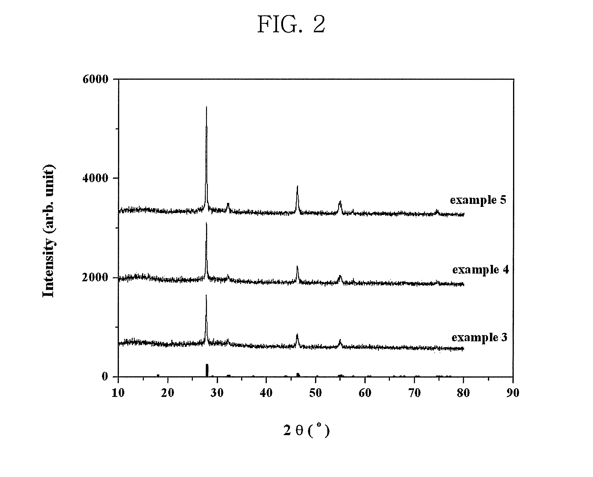
Fabrication of CuInS2 Thin Film (V-CIS-1) Under Vacuum

[0079]Step 1: Fabrication of Copper Thin Film Under Vacuum

[0080]The copper thin film was fabricated in the same manner as the step 1 of Example 1 except that the copper ethylbutyrylacetate precursor was deposited on a glass substrate in the absence of a carrier gas under vacuum at a bubbler temperature of 80° C. to 120° C., a transporting tube temperature of 140° C., and a substrate temperature of 310° C. In the case where the deposition is carried out under vacuum at 350° C. or higher, there is a risk that copper oxide creates on the copper thin film. For this reason, the substrate temperature was maintained to 310° C. The deposition was carried out at a pressure of 1×10⁻³ torr for 3 hours.

[0081]Step 2: Fabrication of CuInS2 Thin Film Under Vacuum

[0082]A CuInS2 thin film was fabricated in the same manner as Example 1 except that the deposition of the CuInS2 thin film in the step 2 of Example 1 was carried out in the absence of a...


PUM

PropertyMeasurementUnit
thicknessaaaaaaaaaa
temperatureaaaaaaaaaa

Abstract

Disclosed is a method for fabricating a CuInS2 thin film by metal-organic chemical vapor deposition (MOCVD). The method comprises fabricating a copper thin film by depositing an asymmetric copper precursor on a substrate by MOCVD and fabricating a CuInS2 thin film by depositing an indium-sulfur-containing precursor on the copper thin film by MOCVD. The method enables fabrication of a CuInS2 thin film with a constant composition even under vacuum as well as an argon (Ar) atmosphere. Disclosed is further a CuInS2 thin film fabricated by the method. Disclosed is further a method for fabricating an In2S3 thin film for a window of a solar cell via deposition of an indium-sulfur-containing precursor on the CuInS2 thin film by MOCVD. Disclosed further is an In2S3 thin film fabricated by the method. The In2S3 thin film is useful for a substitute for CdS conventionally used for windows of solar cells and contributes to simplification in fabrication process of solar cells.

Description

[0001]This non-provisional application claims priority under 35 U.S.C. §119(a) on Korean Patent Application No. 10-2006-0066427 filed on Jul. 14, 2006, which is herein incorporated by reference.BACKGROUND OF THE INVENTION[0002]1. Field of the Invention[0003]The present invention relates to a method for fabricating a CuInS2 thin film by metal-organic chemical vapor deposition (hereinafter, referred to as simply “MOCVD”), a CuInS2 thin film fabricated by the method and a method for fabricating an In2S3 thin film from the CuInS2 thin film. More specifically, the present invention relates to a method for fabricating a CuInS2 thin film, the method comprising fabricating a copper thin film by depositing an asymmetric copper precursor on a substrate by MOCVD and fabricating a CuInS2 thin film by depositing an indium-sulfur-containing precursor on the copper thin film by MOCVD. Furthermore, the present invention relates to a method for fabricating an In2S3 thin film for a window of a solar ...

Claims


Application Information

Patent Timeline
Patent Type & Authority Patents(United States)
IPC IPC(8): C23C16/00C23C16/06
CPCC23C16/305H01L31/0322Y02E10/541
Inventor SHIM, IL WUNLEE, SEUNG SOOSEO, KOOK WONPARK, JONG PIL
Owner SAMSUNG SDI CO LTD
Learn More