Barrier layer for thick film dielectric electroluminescent displays
a dielectric electroluminescent display and barrier layer technology, applied in the direction of discharge tube luminescnet screens, instruments, natural mineral layered products, etc., can solve the problems of volume reduction, functional degradation, and the inability to completely fill the pores of sintered materials of the thick layer, so as to minimize internal stress and minimize internal stress
- Summary
- Abstract
- Description
- Claims
- Application Information
AI Technical Summary
Benefits of technology
Problems solved by technology
Method used
Image
Examples
example 1
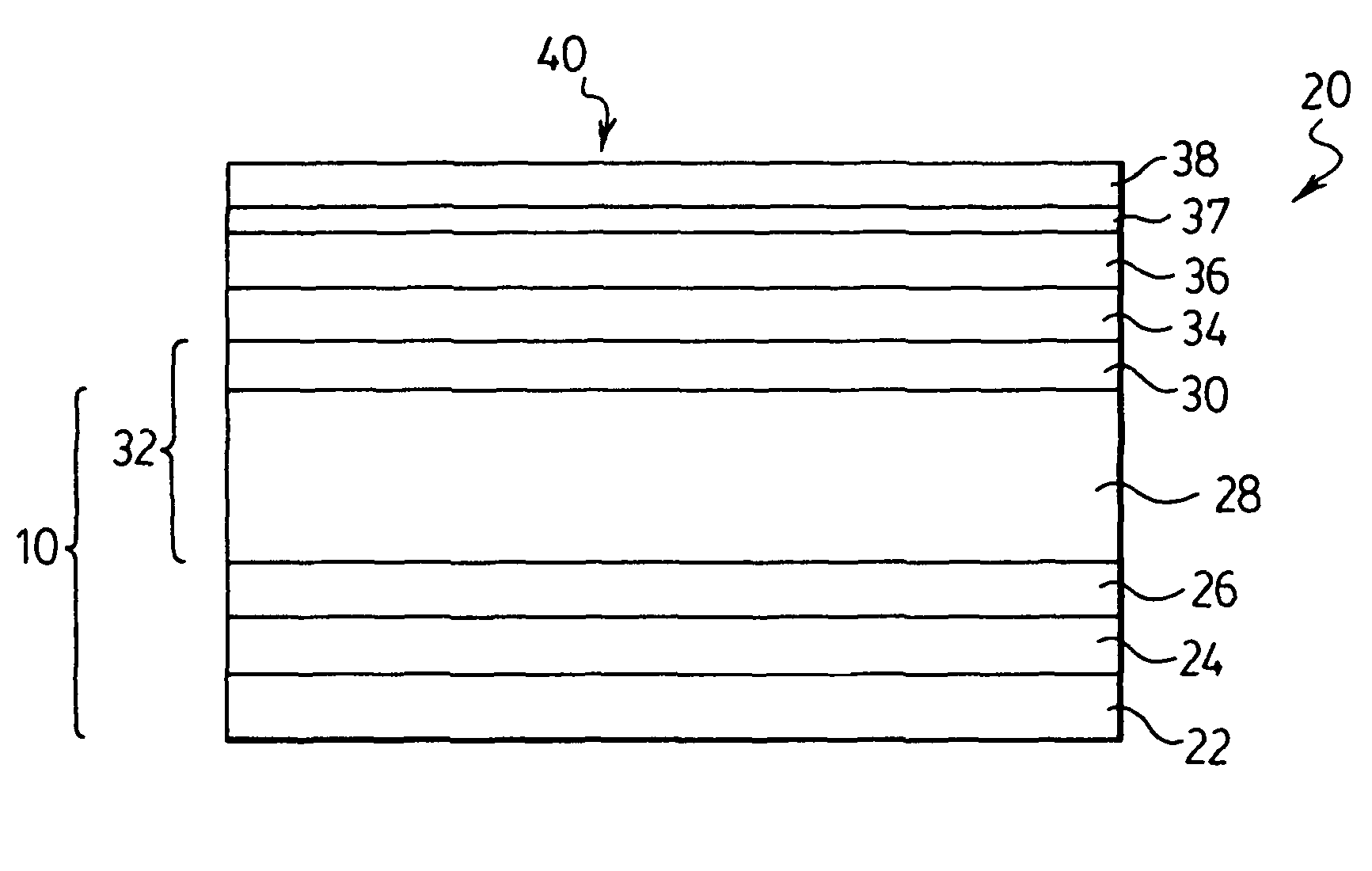
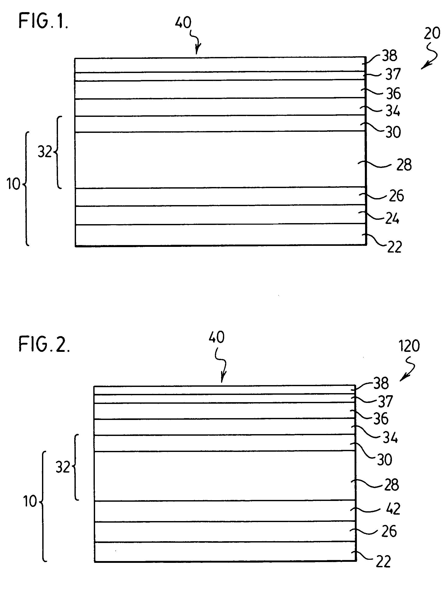
[0107]A thick film dielectric electroluminescent display of the type generally shown in FIG. 1 was fabricated.
[0108]The thick film dielectric electroluminescent display was constructed on a 5 centimeter by 5 centimeter by 1.8 millimeter thick PD200 glass substrate obtained from Asahi Glass of Hillsboro, Oreg., USA onto which was deposited a 2000 Angstrom thick barrier layer of alumina (Al2O3). The alumina was deposited using rf magnetron sputtering in an oxygen / argon mixture at a pressure of 6 millitorr (0.8 Pa). The oxygen to argon ratio was set by admitting argon to the sputtering chamber at a rate of 50 sccm and oxygen at a rate of 2 sccm, with the pumping rate set to maintain the noted pressure. The power supplied to the sputtering target was 2 kW (or 4.4 Watts per square centimeter).
[0109]A 0.8 micrometer thick gold electrode film was formed on the coated substrate by printing and firing TR1207 gold-containing paste from Tanaka Kikinzoku International of Tokyo, Japan. Next, a c...
example 2
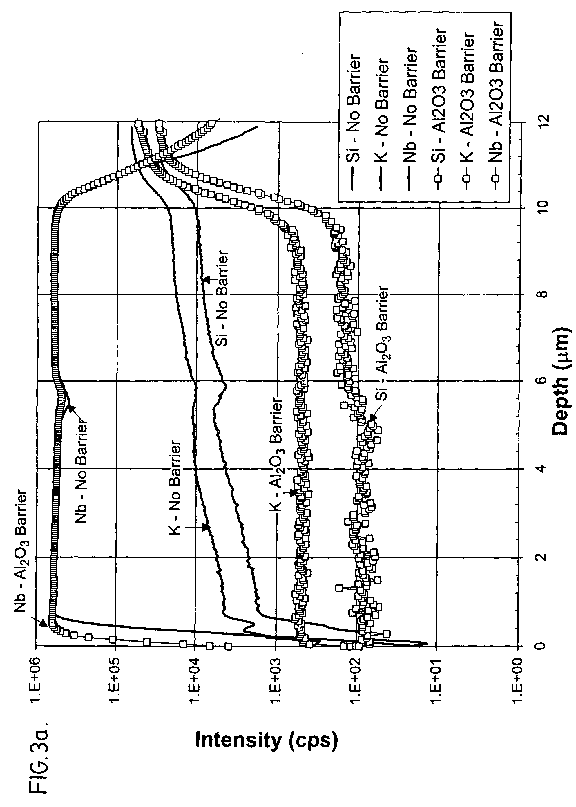
[0114]A thick film dielectric electroluminescent display similar to Example 1 was fabricated, except that no alumina barrier layer was deposited on the glass substrate. The completed display was tested using the test procedure defined in Example 1. The luminance was about 2200 candelas per square meter, which is lower than that for Example 1. It is thought that the lower luminance is due to a lower effective relative dielectric constant of the composite thick film dielectric layer due to diffusion of chemical species from the glass substrate to the composite thick film dielectric layer.
example 3
[0115]A thick film dielectric electroluminescent display similar to Example 1 was fabricated, except that it was fabricated on a 16.9 centimeter by 21.3 centimeter glass substrate. The lower electrode was patterned using photolithographic processing into 0.8 micrometer thick address line strips 495 microns wide separated by 45 micron spaces and the upper electrode was patterned into strips 5 millimeters wide separated by 5 millimeter spaces. The display was tested by connecting the lower address line strips in parallel, and one of the upper electrode strips and then using the test method of Examples 1. The luminance was about 2550 candelas per square meter.
PUM
| Property | Measurement | Unit |
|---|---|---|
| thickness | aaaaa | aaaaa |
| thickness | aaaaa | aaaaa |
| relative dielectric constant | aaaaa | aaaaa |
Abstract
Description
Claims
Application Information
 - R&D
- Intellectual Property
- Life Sciences
- Materials
- Tech Scout
- Unparalleled Data Quality
- Higher Quality Content
- 60% Fewer Hallucinations
Browse by: Latest US Patents, China's latest patents, Technical Efficacy Thesaurus, Application Domain, Technology Topic, Popular Technical Reports.
© 2025 PatSnap. All rights reserved.Legal|Privacy policy|Modern Slavery Act Transparency Statement|Sitemap|About US| Contact US: help@patsnap.com


