Etching method, pattern forming process, thin-film transistor fabrication process, and etching solution
a technology of pattern forming and etching solution, which is applied in the direction of semiconductor devices, electrical devices, chemistry apparatus and processes, etc., can solve the problems of low heat resistance of photoresists that melt and deform, and achieve high selectivity, improve stability and uniformity, and prevent device characteristics from scattering
- Summary
- Abstract
- Description
- Claims
- Application Information
AI Technical Summary
Benefits of technology
Problems solved by technology
Method used
Image
Examples
example 1
Measurement of Etch Rate
[0078]In Example 1, the etching methods of the present invention for etching amorphous oxide films including IZO, IGZO, IGO and ITO will be demonstrated. The following Examples are described under preferable conditions within the scope of the present invention.
[0079]First, samples for experiment were prepared according to the procedure as described below.
[0080]To examine the etch rates of an IGZO film, an IZO film and an IGO film, Si substrates (525 μm in thickness) on each of which an oxide film of 100 nm in thickness was formed were used as substrate members. These oxide films function as etching stoppers. Specifically, three Si substrates were prepared for use. Then, on each Si substrate, an oxide semiconductor film composed of any one of the IGZO film, the IZO film and the IGO film was formed under the conditions as shown in Table 1 by the reactive sputtering as described in the following publication: Applied Physics Letters, 11 Sep. 2006, Vol. 89, No. 11...
example 2
Selective Etching
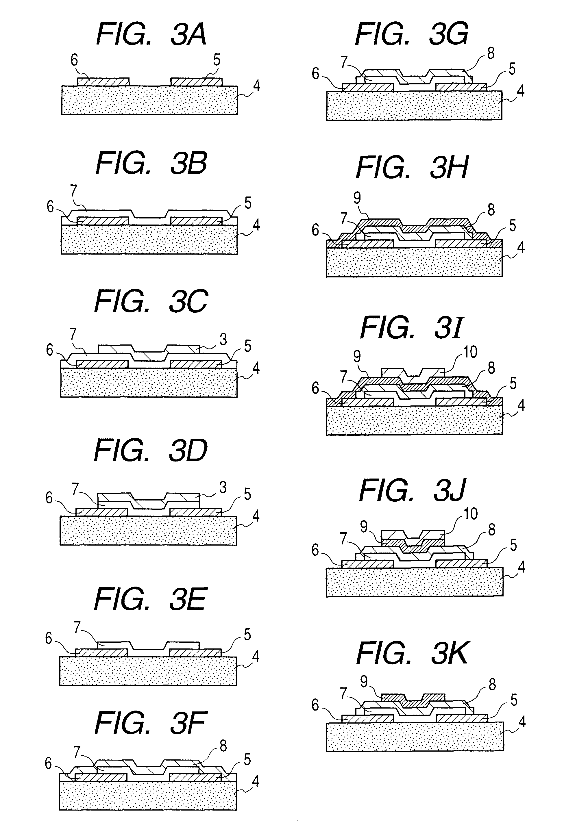
[0094]FIGS. 7A and 7B are a diagrammatic sectional view to illustrate a selective-etching method according to Example 2 of the present invention. In FIGS. 7A and 7B, reference numeral 1 denotes a material layer having a relatively low etch rate; and 2, a material layer having a relatively high etch rate. Reference numeral 3 denotes a resist layer which serves as an etching mask. Where the material layers 1 and 2 each have a low etching selectivity, the excess etch depth Δd of the material layer 1 becomes close to the undercut level Δw of the material layer 2. Where a thin-film transistor using such a structure is fabricated, the problem of scattering is raised in that the thin-film transistor has non-uniform characteristics.
[0095]An ITO layer is used as the material layer 1 and at least one selected from the group consisting of IZO, IGZO and IGO is used to form the material layer 2, so that the etching selectivity of the material layer 2 to the material layer 1 can ...
PUM
 Abstract
Description
Claims
Application Information
 - R&D
- Intellectual Property
- Life Sciences
- Materials
- Tech Scout
- Unparalleled Data Quality
- Higher Quality Content
- 60% Fewer Hallucinations
Browse by: Latest US Patents, China's latest patents, Technical Efficacy Thesaurus, Application Domain, Technology Topic, Popular Technical Reports.
© 2025 PatSnap. All rights reserved.Legal|Privacy policy|Modern Slavery Act Transparency Statement|Sitemap|About US| Contact US: help@patsnap.com


