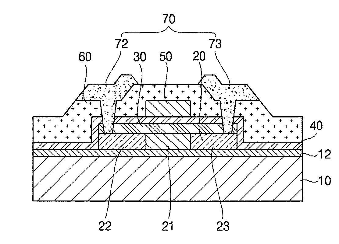
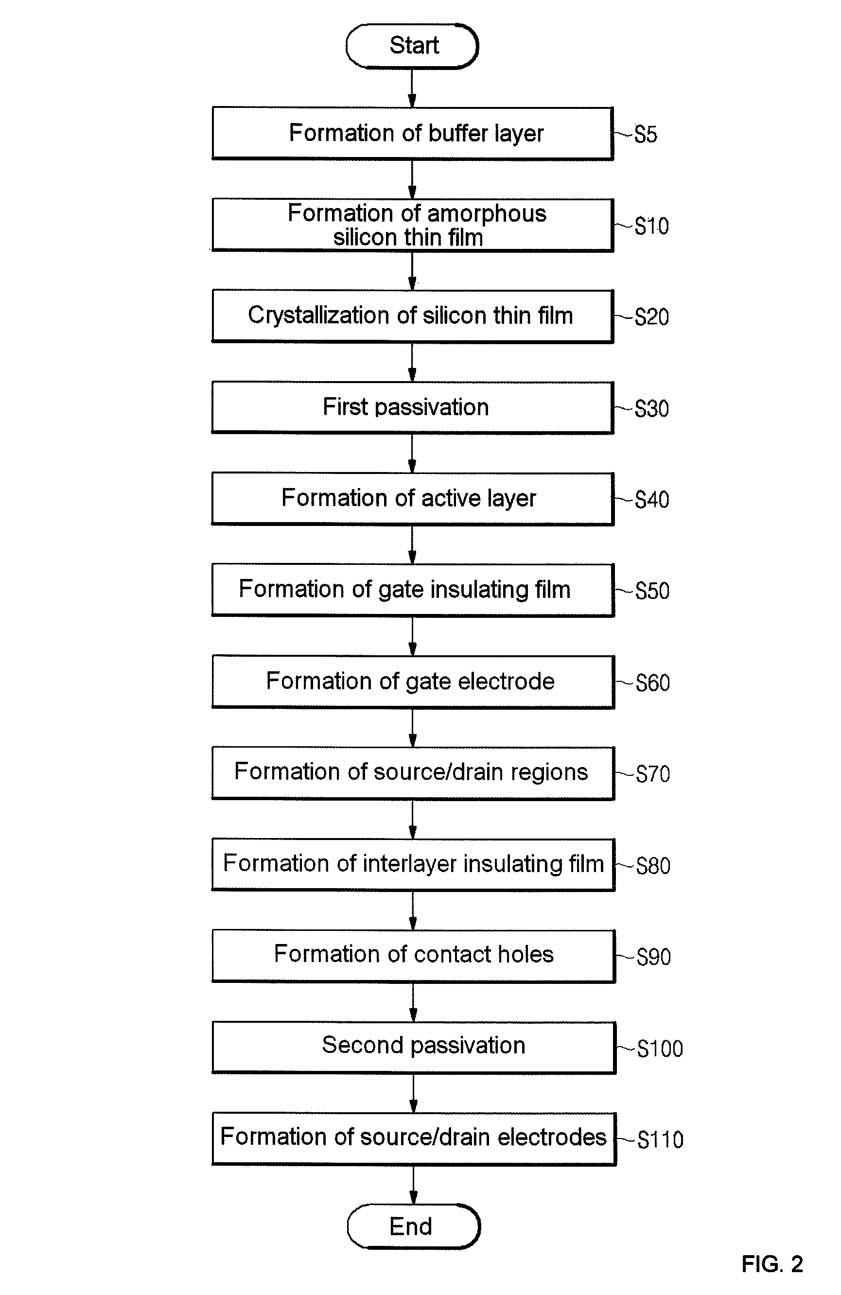
Method for manufacturing thin film transistor
a thin film transistor and manufacturing method technology, applied in the direction of basic electric elements, electrical apparatus, semiconductor devices, etc., can solve the problems of affecting the current characteristics of devices using polycrystalline silicon thin films, and affecting the electron migration of electrons. , to achieve the effect of improving current characteristics and high electron mobility
- Summary
- Abstract
- Description
- Claims
- Application Information
AI Technical Summary
Benefits of technology
Problems solved by technology
Method used
Image
Examples
example 1
[0093]The amorphous silicon thin films were crystallized at different temperatures to form polycrystalline silicon thin films. To clearly observe the temperature-dependent crystallization of the amorphous silicon thin films, the annealing time was decreased with increasing annealing temperature. The annealing of the amorphous silicon thin films was performed under the following sets of temperature / time conditions: 600° C. / 150 minutes (Example 1a), 650° C. / 80 minutes (Example 1b), 700° C. / 20 minutes (Example 1c), 750° C. / 10 minutes (Example 1d), and 800° C. / 5 minutes (Example 1e). The metal catalyst was doped at the same concentration (2×10¹³ / cm2).
example 2
[0094]In this example, the amorphous silicon thin films were crystallized for different periods of time while maintaining the annealing temperature constant to form polycrystalline silicon thin films. Specifically, the amorphous silicon thin films were annealed at 700° C. for 5 minutes (Example 2a), 10 minutes (Example 2b), 20 minutes (Example 2c) and 40 minutes (Example 2d). The metal catalyst was doped at the same concentration (2×10¹³ / cm2).
example 3
[0095]In this example, the amorphous silicon thin films were crystallized by doping the metal catalyst at different concentrations while maintaining the annealing temperature and time constant. Specifically, the metal catalyst was doped at different concentrations: 5×10¹¹ / cm2 (Example 3a), 2×10¹² / cm2 (Example 3b), 2×10¹³ / cm2 (Example 3c), 6×10¹⁴ / cm2 (Example 3d) and 5×10¹⁵ / cm2 (Example 3e). The doped amorphous silicon thin films were annealed at the same temperature (750° C.) for the same period of time (5 minutes) to form polycrystalline silicon thin films.
[0096]The results obtained after the annealing of the amorphous silicon thin films under the different crystallization conditions in Examples 1-3 were evaluated as follows.
[0097]Each of the polycrystalline silicon thin films was etched. The morphology of grain boundaries of the etched thin film was observed. When a general polycrystalline silicon thin film is etched, a metal silicide present at grain boundaries of the polycrystal...
PUM
| Property | Measurement | Unit |
|---|---|---|
| temperature | aaaaa | aaaaa |
| temperature | aaaaa | aaaaa |
| temperature | aaaaa | aaaaa |
Abstract
Description
Claims
Application Information
 - R&D
- Intellectual Property
- Life Sciences
- Materials
- Tech Scout
- Unparalleled Data Quality
- Higher Quality Content
- 60% Fewer Hallucinations
Browse by: Latest US Patents, China's latest patents, Technical Efficacy Thesaurus, Application Domain, Technology Topic, Popular Technical Reports.
© 2025 PatSnap. All rights reserved.Legal|Privacy policy|Modern Slavery Act Transparency Statement|Sitemap|About US| Contact US: help@patsnap.com


