
Monolithic vertically integrated composite group III-V and group IV semiconductor device and method for fabricating same

a semiconductor device and composite group technology, applied in the field of semiconductor devices, can solve the problems of more recent generation more space required for their combination, and difficult integration of conventional silicon devices with more recent generations of non-silicon high-voltage devices

Inactive Publication Date: 2011-03-29
INFINEON TECH AMERICAS CORP
View PDF25 Cites 75 Cited by
  • Summary
  • Abstract
  • Description
  • Claims
  • Application Information

AI Technical Summary

Benefits of technology

This approach enables efficient integration of III-V and IV semiconductor devices on a single die, improving performance by reducing parasitic inductances and enhancing matching, resulting in a composite device with improved reliability and efficiency.

Problems solved by technology

Increased diversity in the types of materials used for semiconductor device fabrication have made integration of conventional silicon devices with more recent generations of non-silicon high voltage devices challenging.
Unfortunately, this conventional approach to implementing group IV semiconductor devices in combination with non-group IV devices entails several significant drawbacks.
For example, because the separate devices are typically fabricated separately on separate dies, their combination requires more space and is more expensive than if the devices were to be integrated on a single die.
In addition, the requirement that the separate dies be electrically coupled in packaging, typically by wire bonding the dies together, introduces reliability and performance constraints flowing from the physical durability of the bonds, as well as parasitic inductances introduced by the wires themselves that may effectively decouple the separate devices at high switching speeds.
Moreover, because the individual devices are fabricated separately on separate dies, particular pairs or groups of individual devices combined for co-packaging may be less than ideally matched, resulting in sub-optimal performance of the composite device.

Method used


Image

  • Monolithic vertically integrated composite group III-V and group IV semiconductor device and method for fabricating same
  • Monolithic vertically integrated composite group III-V and group IV semiconductor device and method for fabricating same
  • Monolithic vertically integrated composite group III-V and group IV semiconductor device and method for fabricating same

Examples


Embodiment Construction

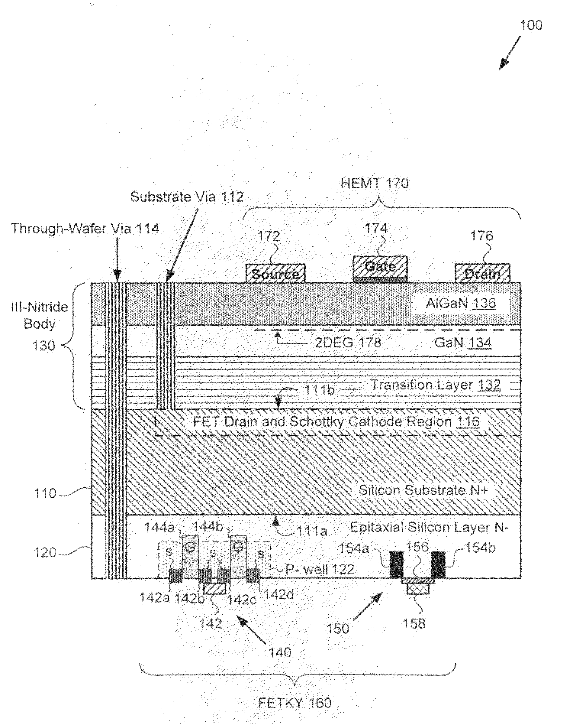
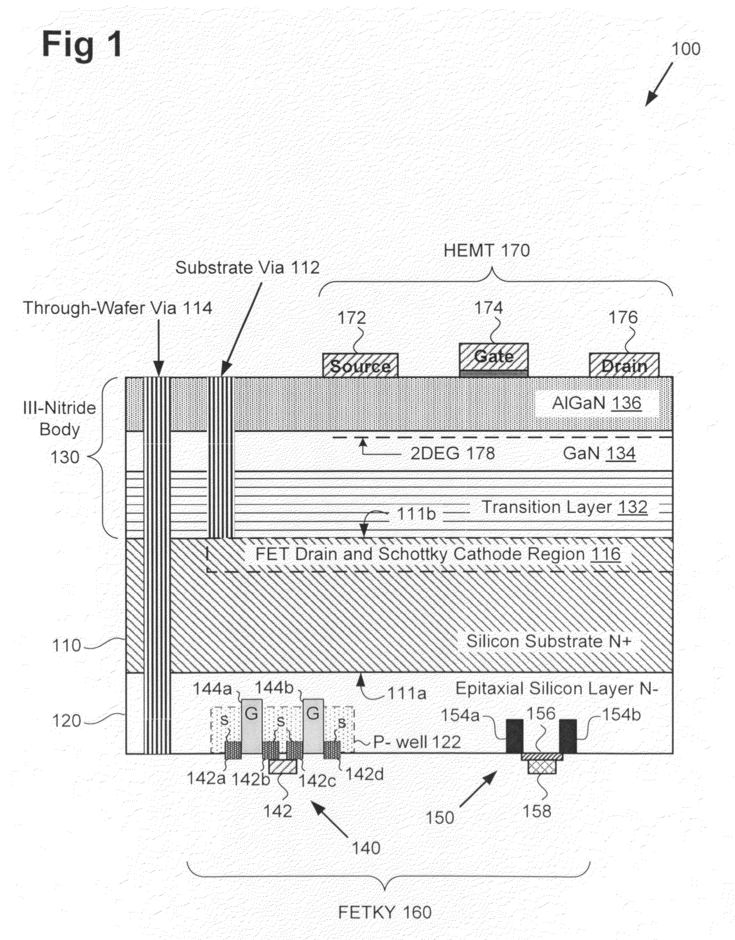
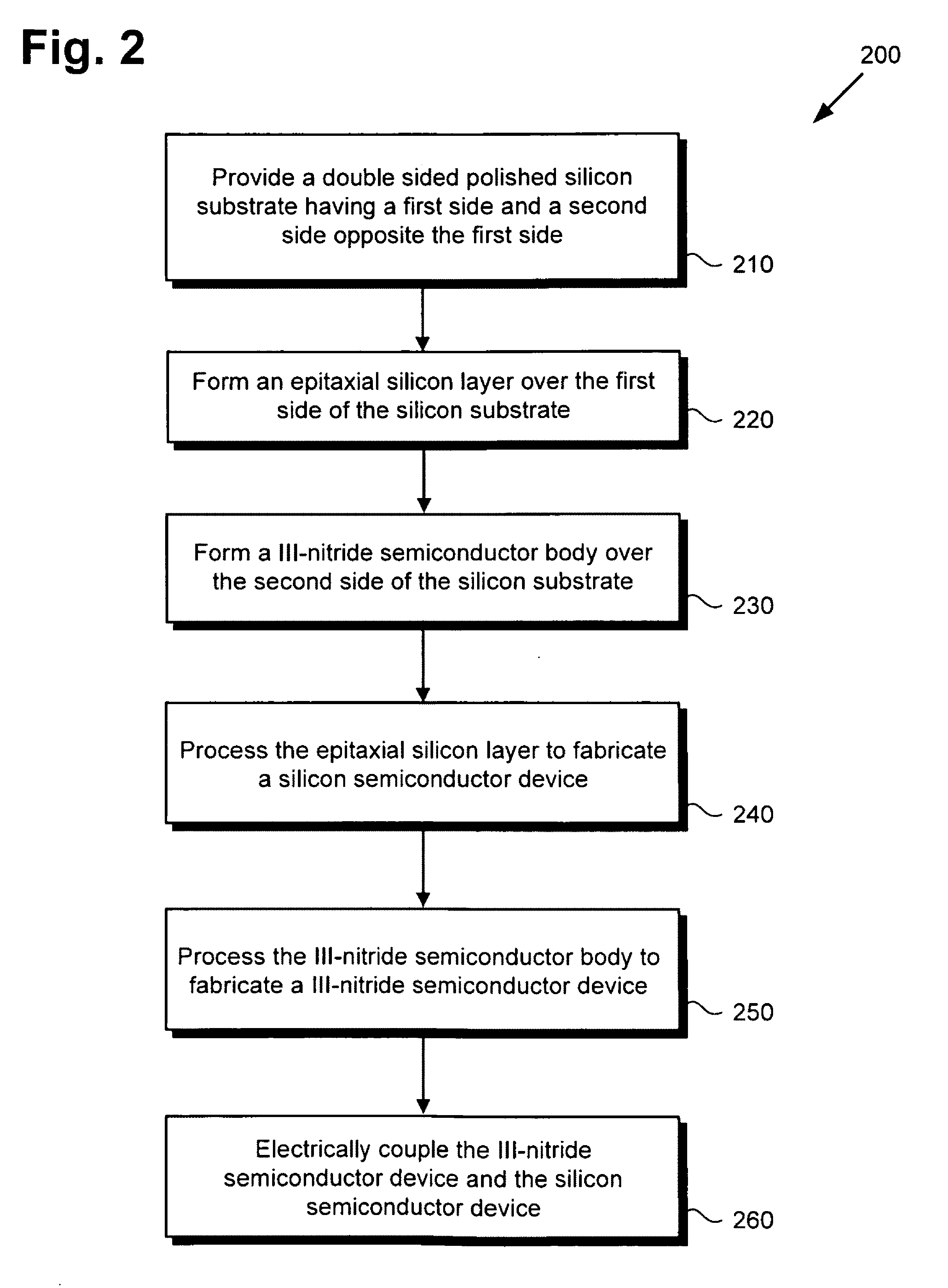
[0013]The present invention is directed to a monolithic vertically integrated composite group III-V and group IV semiconductor device and method for fabricating same. Although the invention is described with respect to specific embodiments, the principles of the invention, as defined by the claims appended herein, can obviously be applied beyond the specifically described embodiments of the invention described herein. Moreover, in the description of the present invention, certain details have been left out in order to not obscure the inventive aspects of the invention. The details left out are within the knowledge of a person of ordinary skill in the art.

[0014]The drawings in the present application and their accompanying detailed description are directed to merely example embodiments of the invention. To maintain brevity, other embodiments of the invention, which use the principles of the present invention, are not specifically described in the present application and are not speci...


PUM


Abstract

According to one disclosed embodiment, a monolithic vertically integrated composite device comprises a double sided semiconductor substrate having first and second sides, a group IV semiconductor layer formed over the first side and comprising at least one group IV semiconductor device, and a group III-V semiconductor body formed over the second side and comprising at least one group III-V semiconductor device electrically coupled to the at least one group IV semiconductor device. The composite device may further comprise a substrate via and / or a through-wafer via providing electric coupling. In one embodiment, the group IV semiconductor layer may comprise an epitaxial silicon layer, and the at least one group IV semiconductor device may be a combined FET and Schottky diode (FETKY) fabricated on the epitaxial silicon layer. In one embodiment, the at least one group III-V semiconductor device may be a III-nitride high electron mobility transistor (HEMT).

Description

BACKGROUND OF THE INVENTION[0001]Definition[0002]In the present application, “group III-V semiconductor” refers to a compound semiconductor that includes at least one group III element and at least one group V element, such as, but not limited to, gallium nitride (GaN), gallium arsenide (GaAs), indium aluminum gallium nitride (InAlGaN), indium gallium nitride (InGaN) and the like. Analogously, “III-nitride semiconductor” refers to a compound semiconductor that includes nitrogen and at least one group III element, such as, but not limited to, GaN, AlGaN, InN, AlN, InGaN, InAlGaN and the like.[0003]1. Field of the Invention[0004]The present invention is generally in the field of semiconductors. More specifically, the present invention is in the field of fabrication of compound semiconductor devices.[0005]2. Background Art[0006]Increased diversity in the types of materials used for semiconductor device fabrication have made integration of conventional silicon devices with more recent g...

Claims


Application Information

Patent Timeline
Patent Type & Authority Patents(United States)
IPC IPC(8): H01L29/739H01L31/072H01L31/109H01L31/0336H01L31/0328
CPCH01L21/8221H01L29/872H01L27/0605H01L27/0694H03K17/567H01L29/205H01L23/535H01L29/78H01L29/778H01L29/2003H01L29/16H01L27/0629H01L29/861H01L29/7786H01L21/8258H01L2924/0002H01L23/481H01L2924/00
Inventor BRIERE, MICHAEL A.
Owner INFINEON TECH AMERICAS CORP
Learn More