Semiconductor device and method for manufacturing the same

a technology of semiconductors and semiconductors, applied in the direction of semiconductor devices, basic electric elements, electrical equipment, etc., can solve the problems of low reliability of devices, and achieve the effect of reducing or preventing the generation of physical stress and improving the reliability of devices

Inactive Publication Date: 2011-02-08
DONGBU HITEK CO LTD
View PDF7 Cites 0 Cited by
  • Summary
  • Abstract
  • Description
  • Claims
  • Application Information

AI Technical Summary

Benefits of technology

[0015]One object of the present invention is to provide a semiconductor device and a method for manufacturing the semiconductor device, which reduces or prevents the generation of a physical stress applied to floating gates and the formation of traps or trap sites on a semiconductor substrate thereby improving the reliability of the device.

Problems solved by technology

Further, when the nitride spacer 60 is formed, traps or trap sites may be formed on the semiconductor substrate 10, which may lower the reliability of the device due to deterioration during annealing.

Method used


Image

  • Semiconductor device and method for manufacturing the same
  • Semiconductor device and method for manufacturing the same
  • Semiconductor device and method for manufacturing the same

Examples


Embodiment Construction

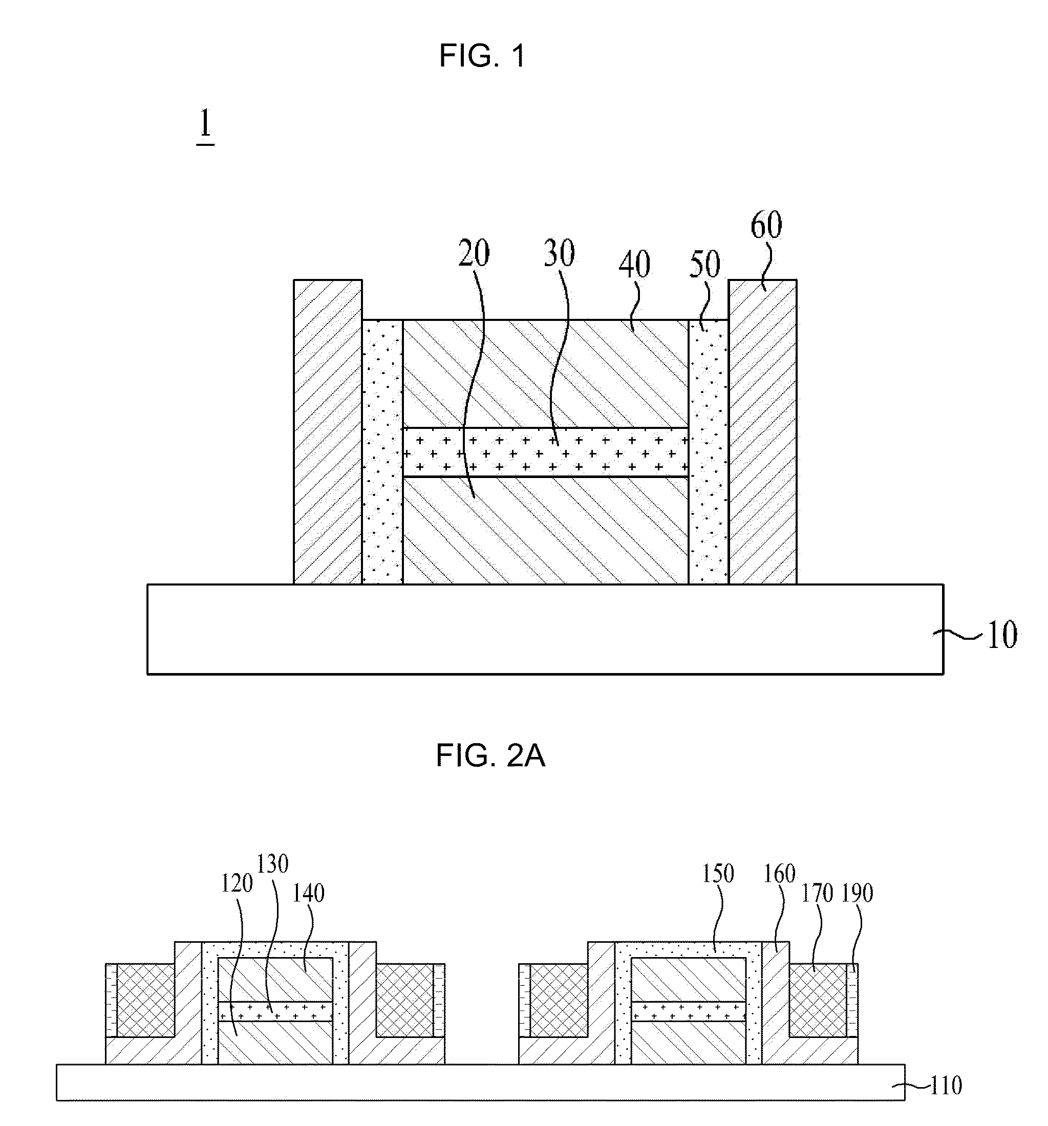
[0023]Reference will now be made in detail to preferred embodiments of the present invention, examples of which are illustrated in the accompanying drawings.

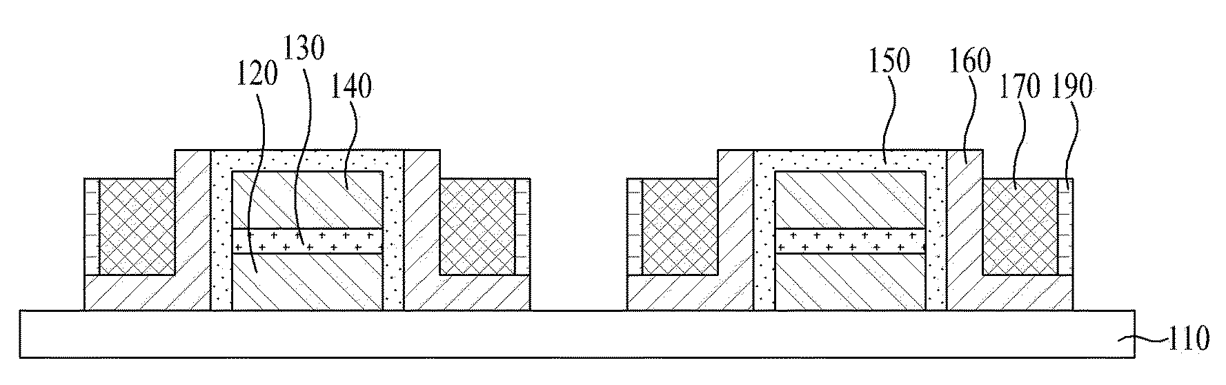
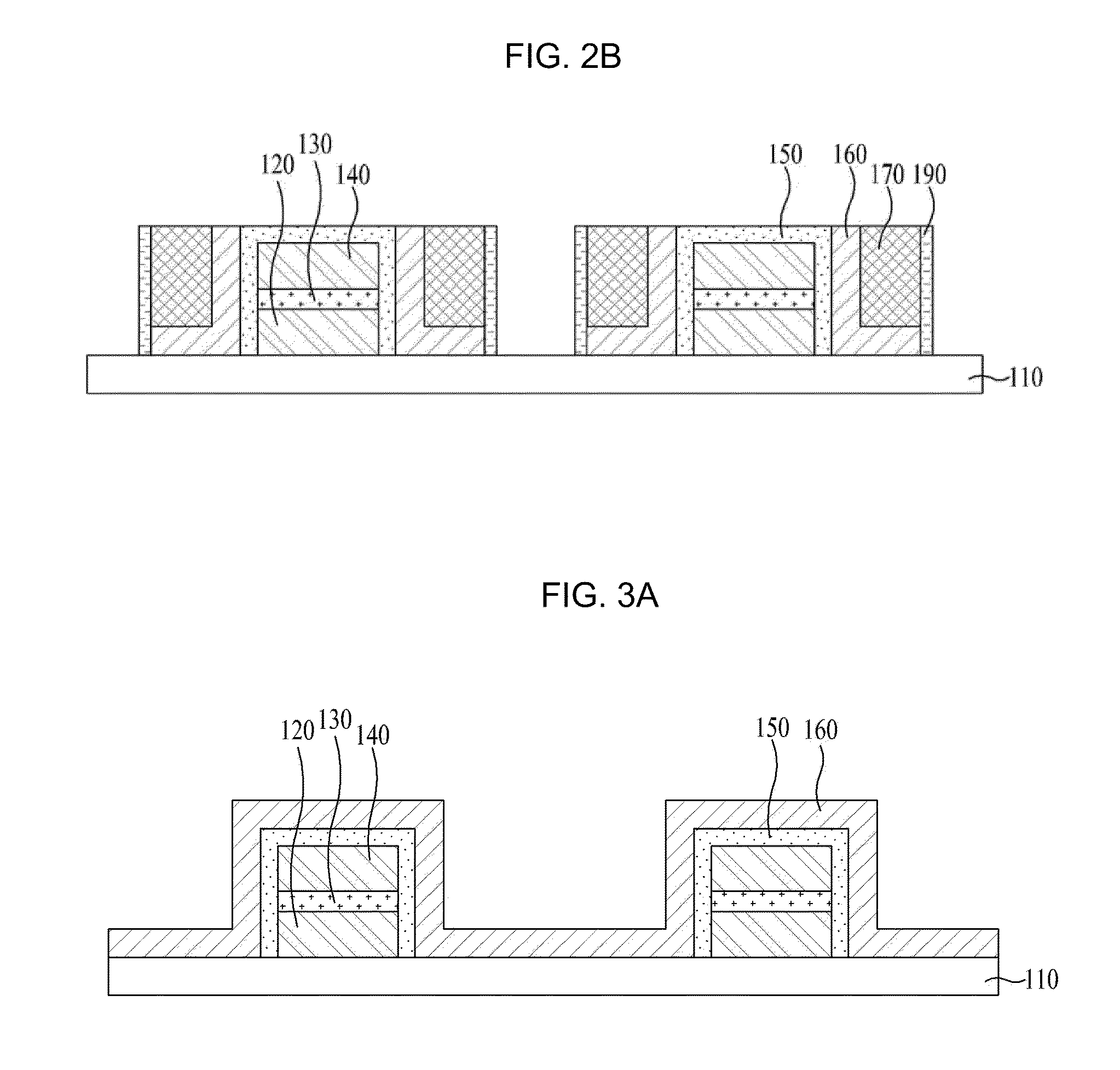
[0024]FIGS. 2A-2B are cross-sectional views of exemplary flash memory devices manufactured by a method in accordance with embodiments of the present invention.

[0025]With reference to FIG. 2A, a flash memory device 100 manufactured by a method in accordance with an embodiment of the present invention includes floating gates 120 formed on a semiconductor substrate 110 to store electric charges, control gates 140 to erase and program the electric charges stored in the floating gates 120, and a tunnel insulating layer 130 (which, in one embodiment, comprises an oxide-nitride-oxide [ONO] trilayer), formed on the floating gates 120, before the control gates 140.

[0026]The flash memory device 100 further includes an oxide layer 150 surrounding the upper surface of the control gates 140 and the side surfaces of the floating and control g...


PUM


Abstract

Disclosed are a semiconductor device and a method for manufacturing the same. The method includes forming a gate layer on a semiconductor substrate; forming a first oxide layer on the semiconductor substrate; forming a second oxide layer on the first oxide layer; exposing the first oxide layer by removing the second oxide layer other than on side surfaces of the gate layer by etching using a photoresist as a mask; and forming junctions in source / drain regions by implanting a high concentration of N-type ions and / or a high concentration of P-type ions using the second oxide layer as a sidewall mask.

Description

[0001]This application claims the benefit of Korean Patent Application No. 10-2007-0130937, filed on Dec. 14, 2007, which is hereby incorporated by reference as if fully set forth herein.BACKGROUND OF THE INVENTION[0002]1. Field of the Invention[0003]The present invention relates to a semiconductor device, and more particularly, to a semiconductor device and a method for manufacturing the same.[0004]2. Discussion of the Related Art[0005]A dynamic random access memory (DRAM) generally includes a cell transistor serving as a switch and a cell capacitor serving as a storage element as components. The DRAM is a volatile random access memory device, which memorizes or erases data through random access to word lines (WL) and bit lines (BL), and loses the data when the power is cut off.[0006]On the other hand, a nonvolatile memory such as a flash memory generally includes only a transistor without a separate capacitor in each cell, different from the DRAM. Such nonvolatile memory is also k...

Claims


Application Information

Patent Timeline
Patent Type & Authority Patents(United States)
IPC IPC(8): H01L21/336
CPCH01L21/28273H01L27/11521H01L29/40114H10B41/30H01L21/67063
Inventor KIM, SUNG JIN
Owner DONGBU HITEK CO LTD
Why Eureka
Try Eureka