Multilayer board and electronic device
a multi-layer board and electronic device technology, applied in the direction of dielectric characteristics, thermoplastic polymer dielectrics, dielectric associations of printed circuit non-printed electric components, etc., can solve the problems of pattern deviation of conductors formed in contact with the multi-layer board, separation of multi-layer boards, etc., to reduce or reduce or prevent the generation of gaps
- Summary
- Abstract
- Description
- Claims
- Application Information
AI Technical Summary
Benefits of technology
Problems solved by technology
Method used
Image

Examples
first preferred embodiment
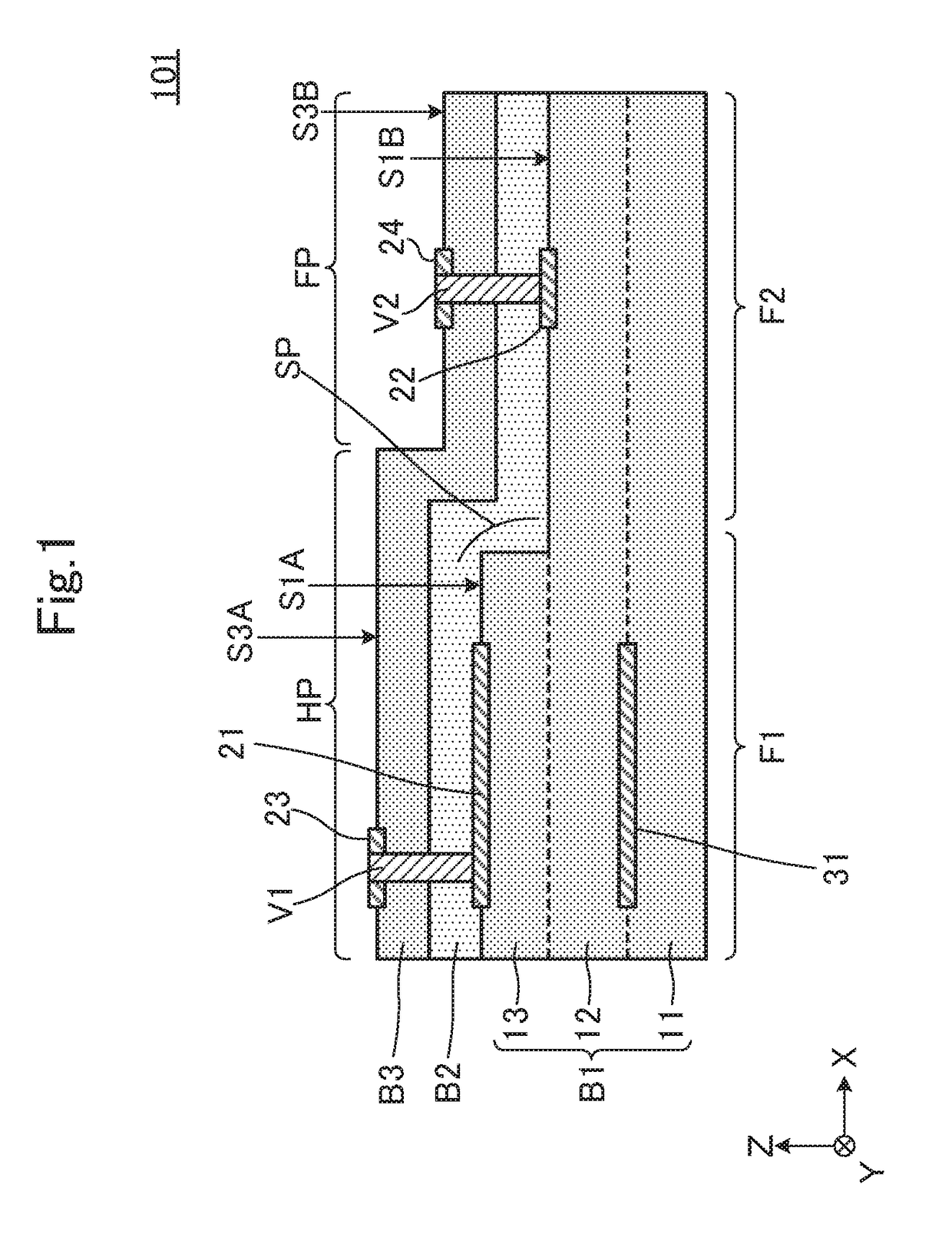
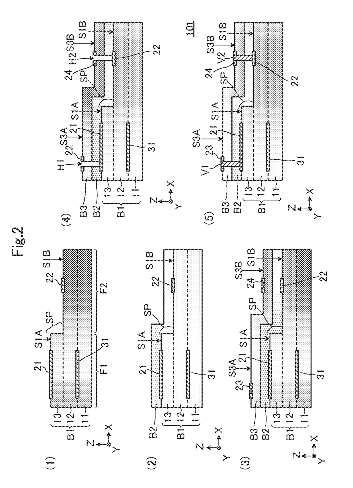
[0029]FIG. 1 is a cross-sectional view of a multilayer board 101 according to a first preferred embodiment of the present invention. It is to be noted that the thickness of each portion is shown in an exaggerated manner in FIG. 1. The same applies to the cross-sectional views shown subsequently.
[0030]The multilayer board 101 includes a first base material substrate B1, a second base material substrate B2, and a third base material substrate B3. The multilayer board 101 is, as shown in FIG. 1, formed by laminating the first base material substrate B1, the second base material substrate B2, and the third base material substrate B3 in this order.
[0031]The first base material substrate B1 is a laminate that preferably has a rectangular or substantially rectangular planar shape and that is formed by laminating a plurality of insulating base material layers 11, 12, 13 which have flexibility, and the laminate includes a first region F1 and a second region F2. As shown in FIG. 1, the first ...
second preferred embodiment
[0055]A second preferred embodiment of the present invention shows an example of a multilayer board without any thick portion or thin portion.
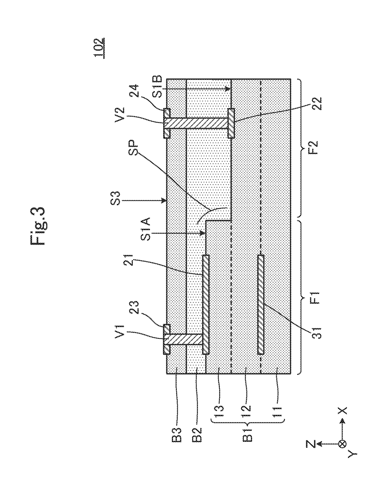
[0056]FIG. 3 is a cross-sectional view of a multilayer board 102 according to the second preferred embodiment.
[0057]The multilayer board 102 differs from the multilayer board 101 according to the first preferred embodiment in the structures of the second base material substrate B2 and the third base material substrate B3. Therefore, the multilayer board 102 includes no thick portion (refer to the thick portion HP in FIG. 1) or thin portion (refer to the thin portion FP in FIG. 1) provided due to a stepped portion SP. The other structure is the same or substantially the same as the multilayer board 101.
[0058]The difference from the multilayer board 101 according to the first preferred embodiment will be described below.
[0059]As shown in FIG. 3, according to the present preferred embodiment, a second base material substrate B2 is laminated on a ...
third preferred embodiment
[0062]A third preferred embodiment of the present invention shows an example of a multilayer board in which a first base material substrate and a third base material substrate partially overlap as viewed in the lamination direction of a plurality of insulating base material layers.
[0063]FIG. 4 is a cross-sectional view of a multilayer board 103 according to the third preferred embodiment.
[0064]The multilayer board 103 differs from the multilayer board 102 in that the second base material substrate B2 is also provided on another portion, in addition to the portion at which the first base material substrate B1 and the third base material substrate B3 overlap with each other, as viewed in the lamination direction of the plurality of insulating base material layers 11, 12, 13 (Z axis direction). In addition, the multilayer board 103 differs from the multilayer board 102 in terms of further including protective layers 1, 2, and other suitable layers. The other structure is the same or su...
PUM
| Property | Measurement | Unit |
|---|---|---|
| thickness | aaaaa | aaaaa |
| elastic modulus | aaaaa | aaaaa |
| conductive | aaaaa | aaaaa |
Abstract
Description
Claims
Application Information
 - R&D
- Intellectual Property
- Life Sciences
- Materials
- Tech Scout
- Unparalleled Data Quality
- Higher Quality Content
- 60% Fewer Hallucinations
Browse by: Latest US Patents, China's latest patents, Technical Efficacy Thesaurus, Application Domain, Technology Topic, Popular Technical Reports.
© 2025 PatSnap. All rights reserved.Legal|Privacy policy|Modern Slavery Act Transparency Statement|Sitemap|About US| Contact US: help@patsnap.com