Solid electrolytic capacitor
a solid electrolytic capacitor and capacitor technology, applied in the manufacture of electrolytic capacitors, capacitor dielectric layers, electrical apparatus casings/cabinets/drawers, etc., can solve the problem of large defective fraction, reduce defective fraction, and reduce defective fraction.
- Summary
- Abstract
- Description
- Claims
- Application Information
AI Technical Summary
Benefits of technology
Problems solved by technology
Method used
Image
Examples
embodiment 1
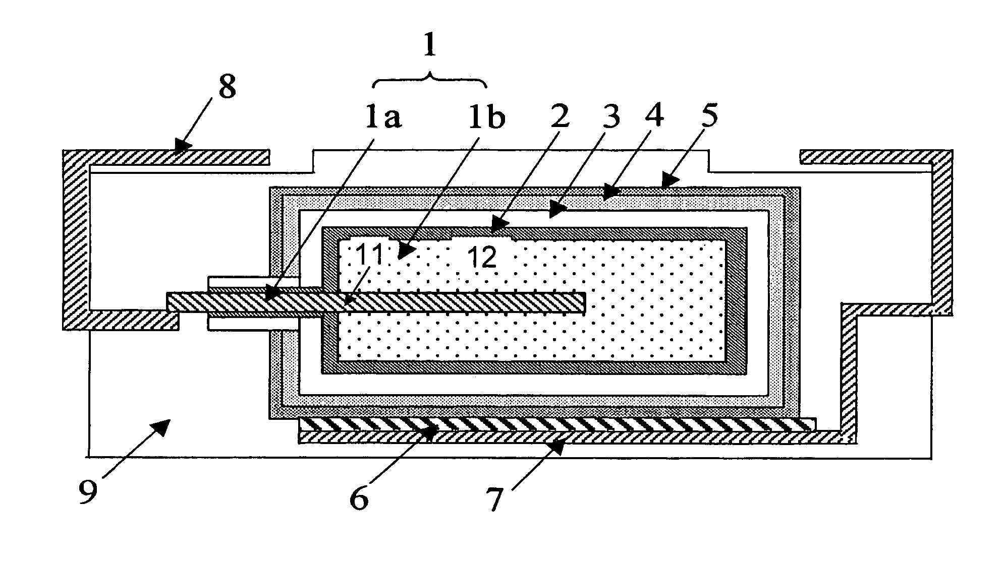
[0044]As an embodiment 1, a sintered porous body 12, metal particles of which have been welded each other by sintering the metal particles having average particle diameter of 2 μm around the anode lead 11 made of niobium (the Vickers hardness at 20 μm from the surface is 30 Hv) with a cooling rate of 0.1° C. / minute in a vacuum is formed. The dimensions of the sintered porous body 12 are about 4 mm in the length, about 3 mm in the width and about 2 mm in the thickness.
[0045]Further, the anode 1 structured by the anode lead 11 and the sintered porous body 12 has been anodized with about 10V of constant voltage for about ten hours in aqueous solution of phosphoric acid of 5 weight-% kept at about 60° C. to form dielectric layer 2 formed by niobium oxide having a thickness of about 25 nm on the surface of the anode 1.
[0046]Next, a conductive high polymer layer 3 composed of polypyrrol is formed on the surface of the dielectric layer 2. Further, carbon paste and silver paste are applied ...
embodiment 2
[0049]In the embodiment 2, the same solid electrolytic capacitor as that of embodiment 1 is formed, except that, as for the anode lead 11 of the embodiment 1, the anode lead 11 structured by niobium (the Vickers hardness is 45 Hv at a point of 20 μm from the surface) with a cooling rate of 0.5° C. / minute is used.
embodiment 3
[0050]In the embodiment 3, the same solid electrolytic capacitor as that of embodiment 1 is formed, except that, as for the anode lead 11 of the embodiment 1, the anode lead 11 structured by niobium (the Vickers hardness is 65 Hv at a point of 20 μm from the surface) with a cooling rate of 1° C. / minute is used.
PUM
| Property | Measurement | Unit |
|---|---|---|
| dielectric constant | aaaaa | aaaaa |
| outer diameter | aaaaa | aaaaa |
| thickness | aaaaa | aaaaa |
Abstract
Description
Claims
Application Information
 - R&D
- Intellectual Property
- Life Sciences
- Materials
- Tech Scout
- Unparalleled Data Quality
- Higher Quality Content
- 60% Fewer Hallucinations
Browse by: Latest US Patents, China's latest patents, Technical Efficacy Thesaurus, Application Domain, Technology Topic, Popular Technical Reports.
© 2025 PatSnap. All rights reserved.Legal|Privacy policy|Modern Slavery Act Transparency Statement|Sitemap|About US| Contact US: help@patsnap.com


