Negative capacity circuit for high frequencies applications

a capacitance circuit and negative technology, applied in the field of negative capacitance circuits, can solve the problem that circuits cannot be used for high frequency applications, and achieve the effect of simple operation

Active Publication Date: 2010-12-14
STMICROELECTRONICS SRL
View PDF20 Cites 24 Cited by
  • Summary
  • Abstract
  • Description
  • Claims
  • Application Information

AI Technical Summary

Benefits of technology

[0007]An embodiment provides a negative capacitance circuit which is simple to carry out and which can be used for RF filters for mobile telecommunications.
[0008]Another embodiment provides a negative capacitance circuit which can be easily combined with filtering circuits based on Bulk Acoustic Wave (B.A.W.) resonators.

Problems solved by technology

However, one may notice that such circuits can not be used for high frequencies applications, operating at frequencies beyond 2 Ghz in BiCMOS technology.

Method used


Image

  • Negative capacity circuit for high frequencies applications
  • Negative capacity circuit for high frequencies applications
  • Negative capacity circuit for high frequencies applications

Examples


Embodiment Construction

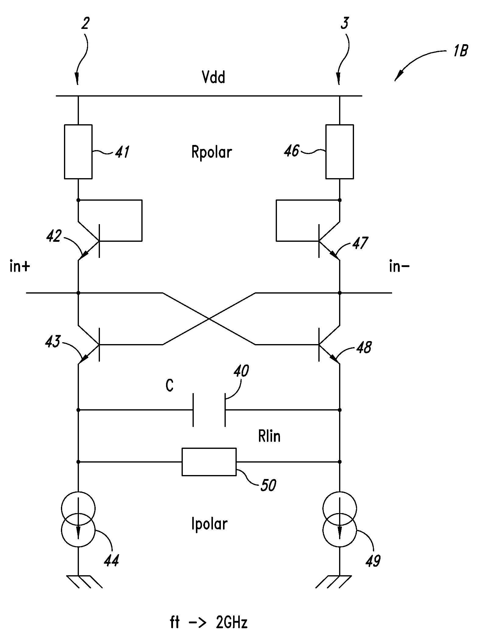
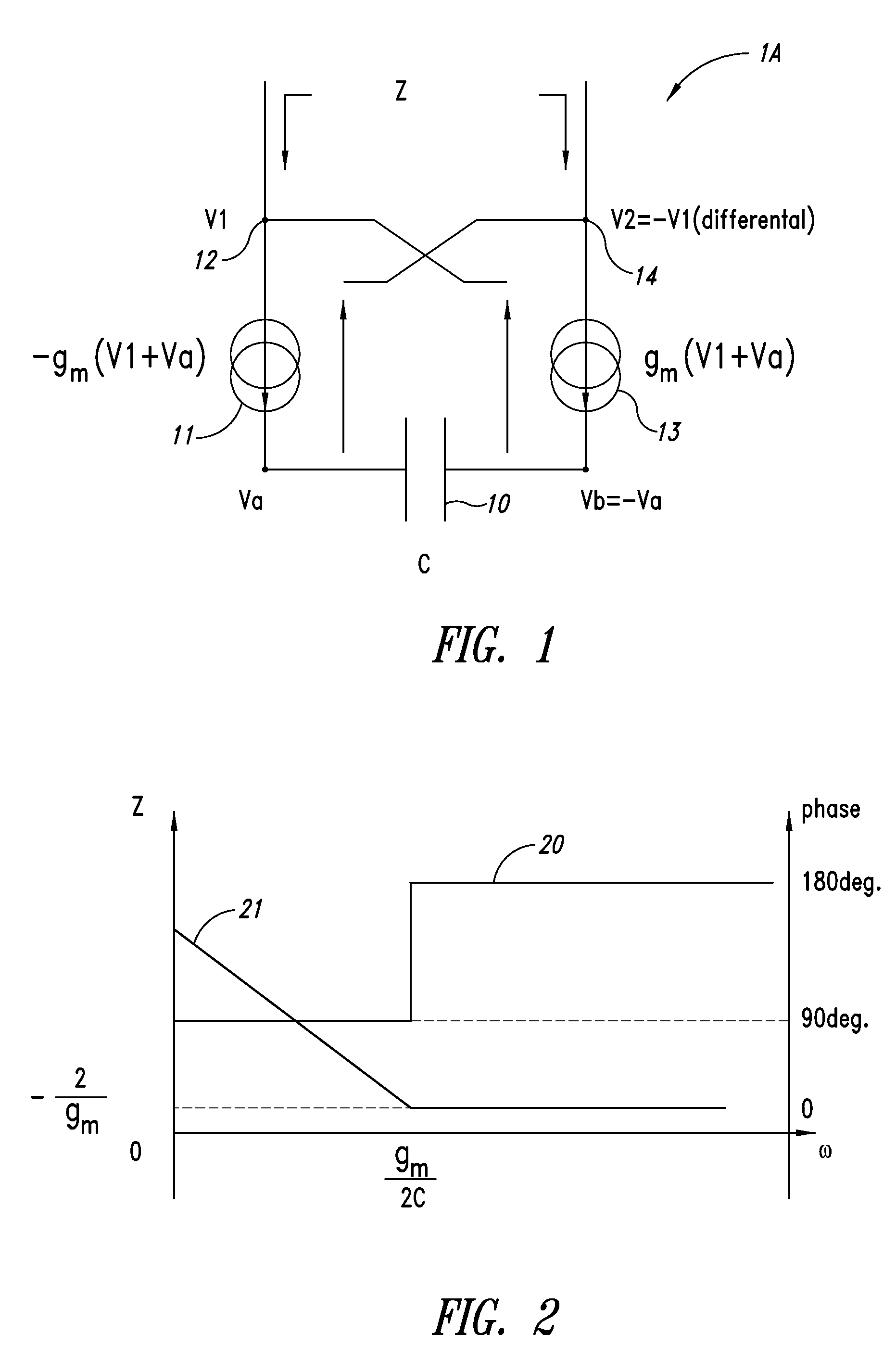
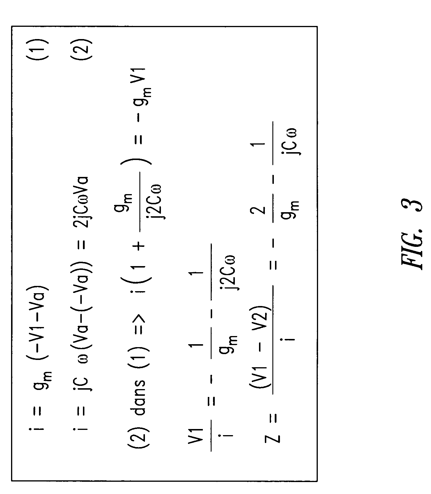
[0035]In the following description, numerous specific details are given to provide a thorough understanding of embodiments. One skilled in the relevant art will recognize, however, that the invention can be practiced without one or more of the specific details, or with other methods, components, materials, etc. In other instances, well-known structures, materials, or operations are not shown or described in detail to avoid obscuring aspects of the invention.

[0036]Reference throughout this specification to “one embodiment” or “an embodiment” means that a particular feature, structure, or characteristic described in connection with the embodiment is included in at least one embodiment. Thus, the appearances of the phrases “in one embodiment” or “in an embodiment” in various places throughout this specification are not necessarily all referring to the same embodiment. Furthermore, the particular features, structures, or characteristics may be combined in any suitable manner in one or m...


PUM


Abstract

A negative capacitances circuit includes first and second branches connected between a first reference voltage and a second reference voltage. The first branch includes, in series, a first biasing resistor, a first diode, a first bipolar transistor, and a first current source. The second branch includes, in series, a second biasing resistor, a second diode, a second bipolar transistor, and a second current source. The first transistor has a base coupled to a collector of the second transistor and to one input, and the second transistor has a base coupled to a collector of the first transistor and to another input. A capacitor is connected between the emitter of said first transistor and the emitter of said second transistor. A linearization resistor is coupled in parallel between the two emitters of said first and said second transistors.

Description

TECHNICAL FIELD[0001]The present disclosure generally relates to the field of electronic circuits and more particularly but not exclusively to a negative capacitance circuit.BACKGROUND INFORMATION[0002]Circuits achieving an electric model being equivalent to a negative capacitor are already known in the art, as shown in the following publications.[0003]The document “Using a negative capacitance to increase the tuning range of a varactor diode in MMIC technology”, Svilen Kolev, IEEE Transactions on microwave theory and techniques, December 2001, discloses a first application of such a negative capacitance circuit.[0004]Another application of such a circuit is disclosed in this publication “Generation of negative capacitance in a common gate MESFET stage and application to optical receiver design at microwave frequencies”, Jason D Drew, Wideband circuits, modeling and techniques, IEE colloquium, May 1996.[0005]However, one may notice that such circuits can not be used for high frequen...

Claims


Application Information

Patent Timeline
Patent Type & Authority Patents(United States)
IPC IPC(8): H03H11/46H03H9/54
CPCH03B5/326H03B5/366H03H11/481
Inventor CATHELIN, ANDREIARAZAFIMANDIMBY, STEPHANETILHAC, CYRILLE
Owner STMICROELECTRONICS SRL
Why Eureka
Try Eureka