
Nonvolatile semiconductor storage device and method for manufacturing same

a storage device and non-volatile technology, applied in semiconductor devices, semiconductor/solid-state device details, electrical equipment, etc., can solve the problems of increasing the bit density of future nand flash memory, reducing reliability, and increasing the fluctuation of transistors

Inactive Publication Date: 2010-12-14
KK TOSHIBA
View PDF8 Cites 96 Cited by
  • Summary
  • Abstract
  • Description
  • Claims
  • Application Information

AI Technical Summary

Benefits of technology

The invention provides a nonvolatile semiconductor storage device with a unique structure and a method for manufacturing it. The device includes a substrate, multiple stacked units, a gate electrode, a charge storage layer, and two insulating films. The spacing between the stacked units is alternating, and the second spacing is provided at a periodic interval four times the size of a half pitch F of the bit line. The charge storage layer is provided between the semiconductor layer and the protruding portion of the gate electrode, and the two insulating films are provided between the charge storage layer and the protruding portion and between the charge storage layer and the gate electrode, respectively. The method includes stacking to form the semiconductor layer and insulating layer film on the substrate, processing them to provide the first and second spacing, and forming the insulating film and gate electrode film on the side face of the stacked unit. The technical effects of the invention include a unique structure that allows for high-density storage and a simplified manufacturing process.

Problems solved by technology

However, bit density increase of future NAND flash memory will face many issues such as limitations on the downscaling of lithography, reduced reliability due to the transistor scaling, increased fluctuation of the transistor characteristics accompanying the transistor size downscaling, limitations on operation speed due to negative effects of downscaling such as short channel effects or narrow channel effects, and so on.
Then, forming the silicon plug after the gate electrode formation constrains the materials used in the gate electrode; and it is difficult to reduce the resistance.

Method used


Image

  • Nonvolatile semiconductor storage device and method for manufacturing same
  • Nonvolatile semiconductor storage device and method for manufacturing same
  • Nonvolatile semiconductor storage device and method for manufacturing same

Examples


first embodiment

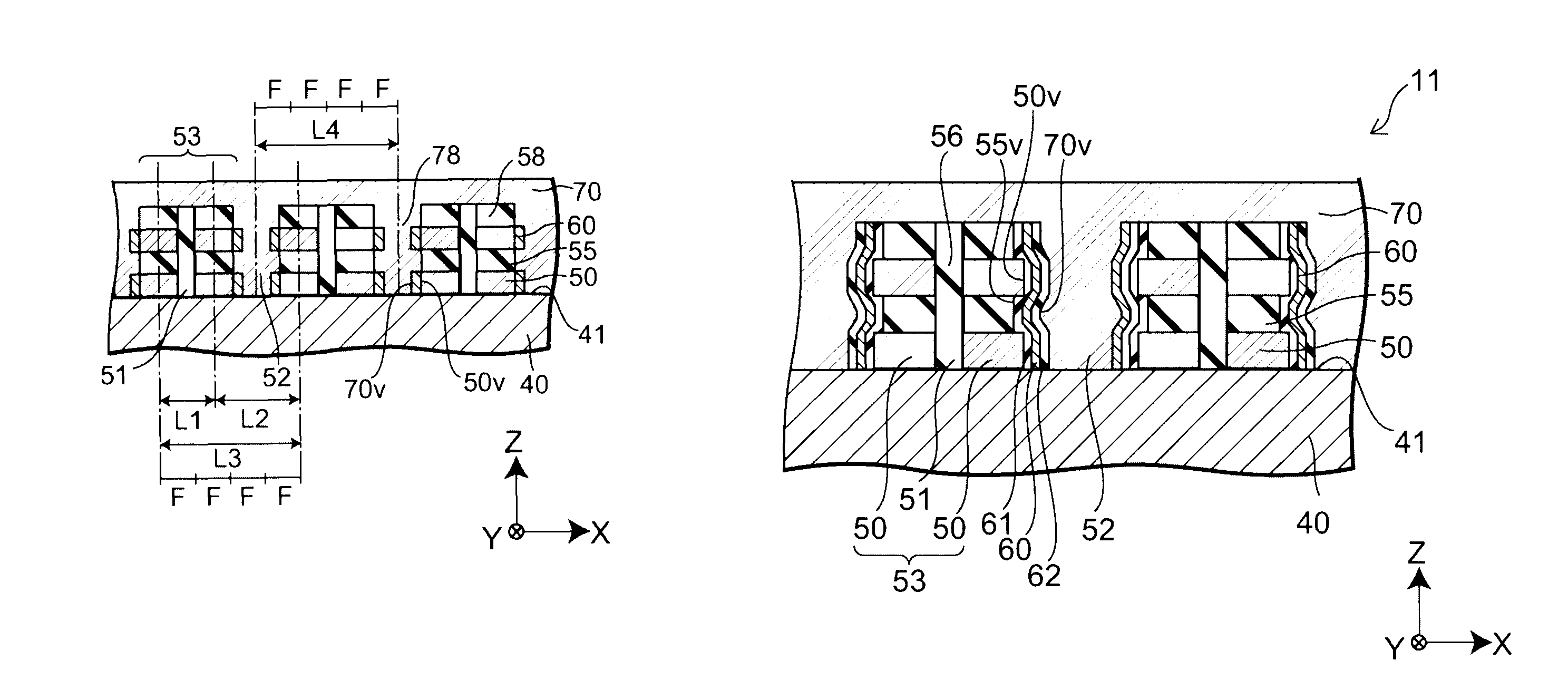
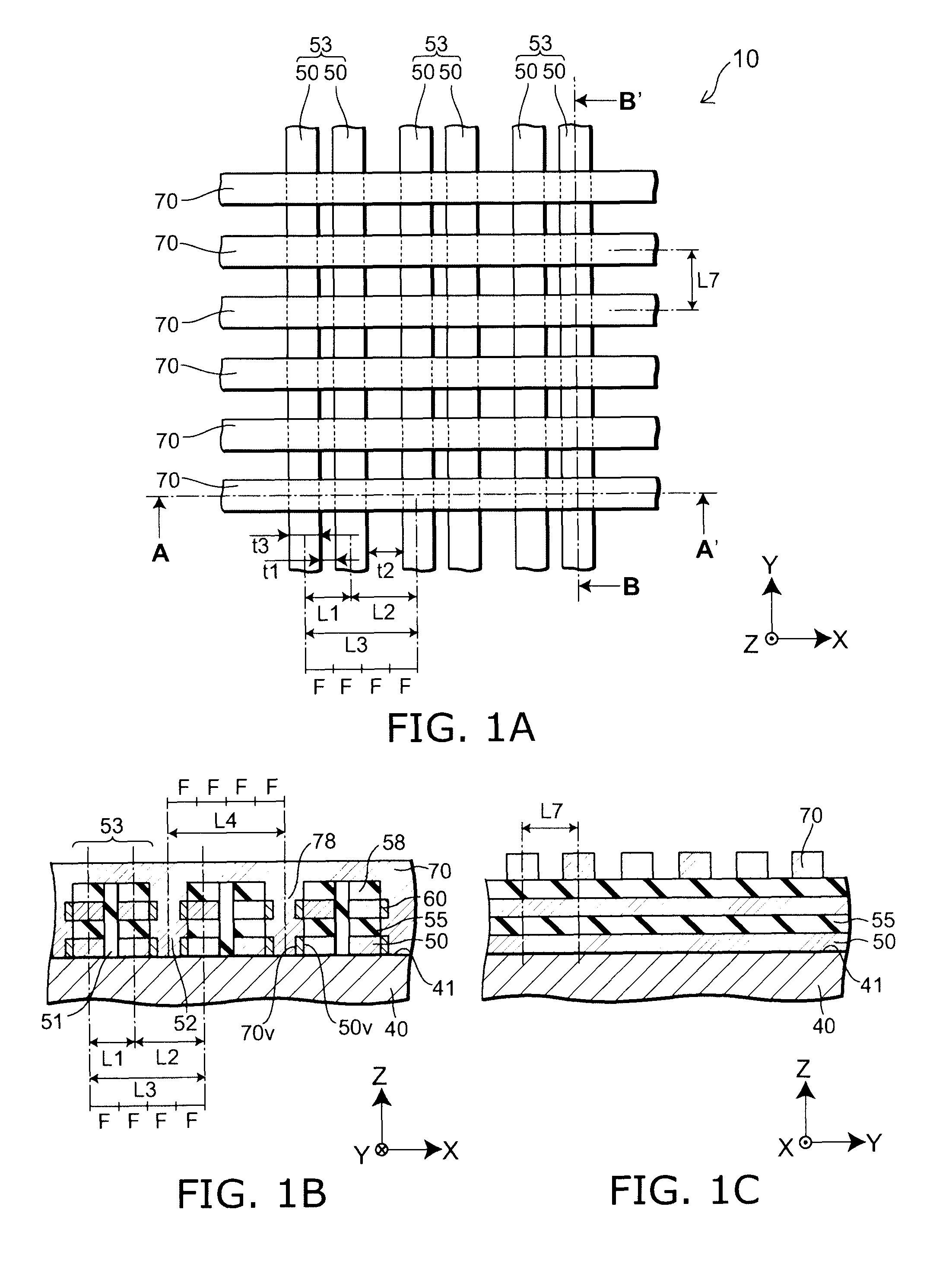
[0026]FIGS. 1A to 1C are schematic views illustrating a configuration of a nonvolatile semiconductor storage device according to a first embodiment of the present invention.

[0027]That is, FIG. 1A is a plan view, FIG. 1B is a cross-sectional view along line A-A′ of FIG. 1A, and FIG. 1C is a cross-sectional view along line B-B′ of FIG. 1A.

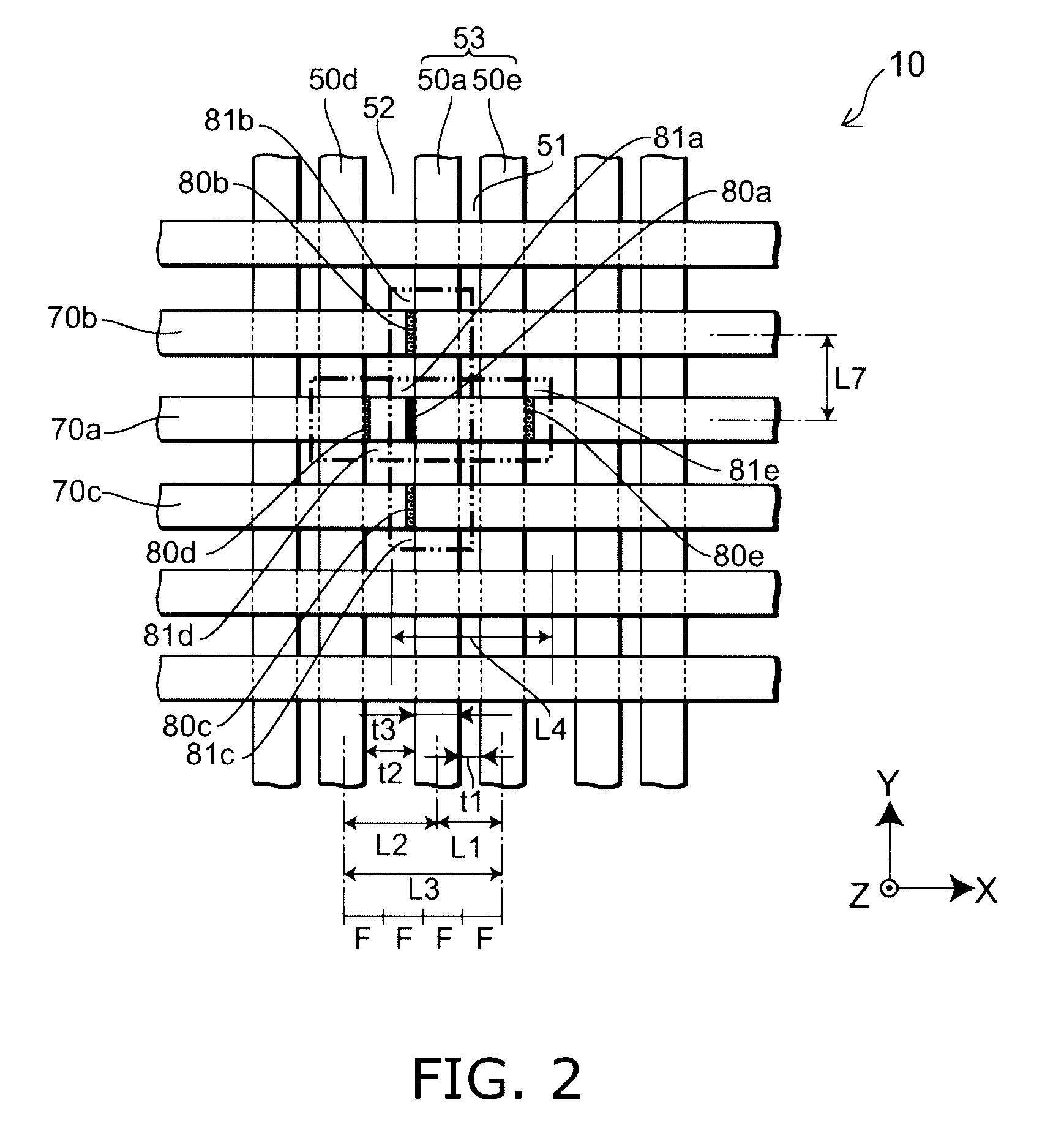
[0028]As illustrated in FIGS. 1A to 1C, a nonvolatile semiconductor storage device 10 according to the first embodiment of the present invention includes a semiconductor layer 50, a gate electrode 70 provided to face the semiconductor layer 50, a charge storage layer 60 provided between the semiconductor layer 50 and the gate electrode 70, a first insulating film (not illustrated) provided between the semiconductor layer 50 and the charge storage layer 60, and a second insulating film (not illustrated) provided between the charge storage layer 60 and the gate electrode 70. In other words, the nonvolatile semiconductor storage device 10 is a memory in...

first example

[0080]A nonvolatile semiconductor storage device 20 according to a first example of the present invention is a flash memory using two stacked layers of memory cells having a 22 nm half pitch to realize a cell surface area of 968 nm2 corresponding to a nonvolatile semiconductor storage device of a conventional planar cell structure having a 15 nm half pitch.

[0081]An insulating layer that separates the substrate 40 and the first semiconductor layer 50 is shared as a gate insulation film of a peripheral high-voltage circuit. Restated, the gate insulation film of a transistor of the peripheral high-voltage circuit includes a layer which forms an insulating layer between the substrate 40 and the semiconductor layer 50 most proximal to the substrate 40. Then, polycrystalline silicon is used as the silicon channel of the semiconductor layer 50. The charge storage layer 60 is formed in the structure illustrated in FIG. 3A. In other words, the charge storage layer 60 is provided separately f...

second example

[0119]A nonvolatile semiconductor storage device 21 according to a second example of the present invention is a five-layer stacked memory corresponding to a 10-nm generation half pitch. The nonvolatile semiconductor storage device 21 is an example in which each monocrystalline silicon film forming the semiconductor layers 50 is formed by a stacked film of a monocrystalline silicon film / oxide film formed by sequentially growing stacks of epitaxial silicon and epitaxial silicon-germanium, removing the silicon-germanium film by selective etching, and performing thermal oxidation of the resulting openings.

[0120]Although the charge storage layer of the first example is separated by reactive ion etching during the patterning of the gate electrode and thermal oxidation of the charge storage layer, the movement of charge is inhibited in this example by making the length of the charge storage layer 60 between cells in the stacking direction longer than the distance between the stacked cells ...


PUM


Abstract

A nonvolatile semiconductor storage device includes: a plurality of stacked units juxtaposed on a major surface of a substrate, each stacked unit aligning in a first direction parallel to the major surface of the substrate; and a gate electrode aligning parallel to the major surface in a second direction non-parallel to the first direction. Each of the plurality of stacked units includes a plurality of stacked semiconductor layers via an insulating layer. The plurality of stacked units are juxtaposed so that the spacings between adjacent stacked units are alternately a first spacing and a second spacing larger than the first spacing. The second spacing is provided at a periodic interval four times a size of a half pitch F of the bit line. The gate electrode includes a protruding portion that enters into a gap of the second spacing between the stacked units. A first insulating film, a charge storage layer, and a second insulating film are provided between a side face of the semiconductor layer and the protruding portion.

Description

CROSS-REFERENCE TO RELATED APPLICATIONS[0001]This application is based upon and claims the benefits of priority from the prior Japanese Patent Application No. 2008-146188, filed on Jun. 3, 2008; the entire contents of which are incorporated herein by reference.BACKGROUND OF THE INVENTION[0002]1. Field of the Invention[0003]The present invention relates to a nonvolatile semiconductor storage device and a method for manufacturing the same.[0004]2. Background Art[0005]Nonvolatile memory typified by NAND flash memory is used widely for large-capacity data storage in mobile telephones, digital still cameras, USB memory, silicon audio, and the like. The market continues to grow due to the reduction of manufacturing costs per bit enabled by rapid downscaling. NAND flash memory in particular has a small cell surface area of 4F2, where F is the minimum processing dimension (the half pitch); and rapid downscaling due to the simple structure thereof is progressing. However, bit density increas...

Claims


Application Information

Patent Timeline
Patent Type & Authority Patents(United States)
IPC IPC(8): H01L23/62
CPCH01L27/11573H01L27/11578H01L27/11582H10B43/40H10B43/20H10B43/27H01L21/28141
Inventor KIYOTOSHI, MASAHIRO
Owner KK TOSHIBA
Learn More