Lateral pocket implant charge trapping devices

a technology of charge trapping device and lateral pocket, which is applied in the direction of digital storage, semiconductor devices, instruments, etc., can solve the problems of non-uniform charge trapping along the way, and achieve the effect of good data retention and fast erase speed

Active Publication Date: 2010-11-23
MACRONIX INT CO LTD
View PDF71 Cites 7 Cited by
  • Summary
  • Abstract
  • Description
  • Claims
  • Application Information

AI Technical Summary

Benefits of technology

[0014]Basically, a memory cell as described herein comprises a first source / drain terminal and a second source / drain terminal having a first conductivity type. The channel between the first and second source / drain terminals has a second conductivity type. The charge trapping structure overlies the channel, and a gate overlies the charge trapping structure. The channel length is defined as the length extending between the first and second source / drain terminals. The channel width is defined as orthogonal to the length extending from a first side to a second side of the channel. A lateral pocket of dopants having the second conductivity type the same as the channel is formed along at least one of the first and second sides of the channel, so that the channel has a profile of concentration of dopants of the second conductivity type that is higher in the lateral pocket than in the central region of the channel. For example, the concentration of dopants in the lateral pocket can be high enough to effectively disable the channel along the sides of the channel.

Problems solved by technology

This greater thickness along the sides results in non-uniform charge trapping along the sides of the charge trapping structure, the effects of which can be reduced or eliminated by the lateral pocket implant.
For example, when an insulation material is along the sides of the channel, the process for making insulation material and the charge trapping structure may result in anomalies, such as bird's beaks, in the charge trapping structure along the sides which are adjacent insulation material.

Method used


Image

  • Lateral pocket implant charge trapping devices
  • Lateral pocket implant charge trapping devices
  • Lateral pocket implant charge trapping devices

Examples


Embodiment Construction

[0045]A detailed description of embodiments of the present invention is provided with reference to the FIGS. 1 through 18a-18c.

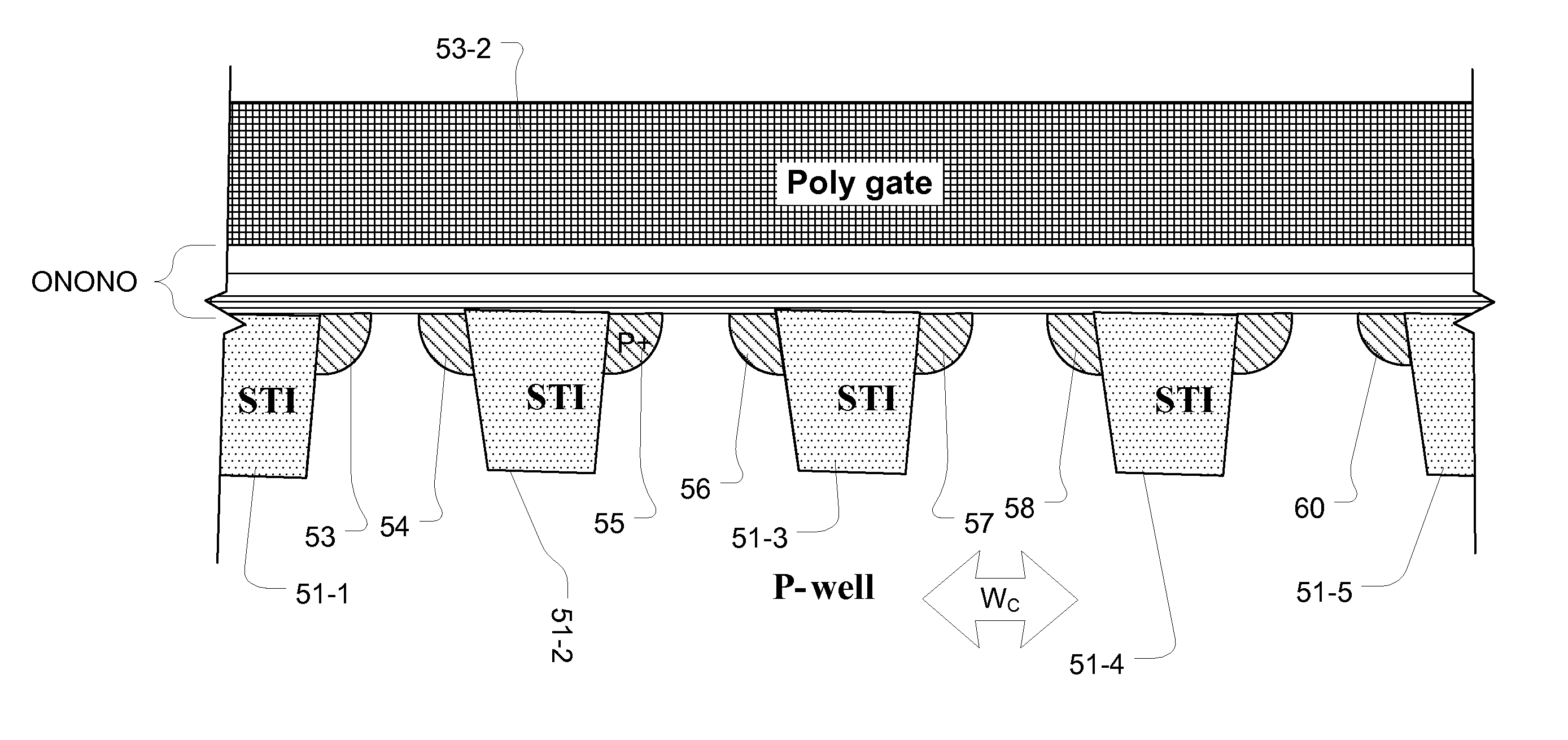
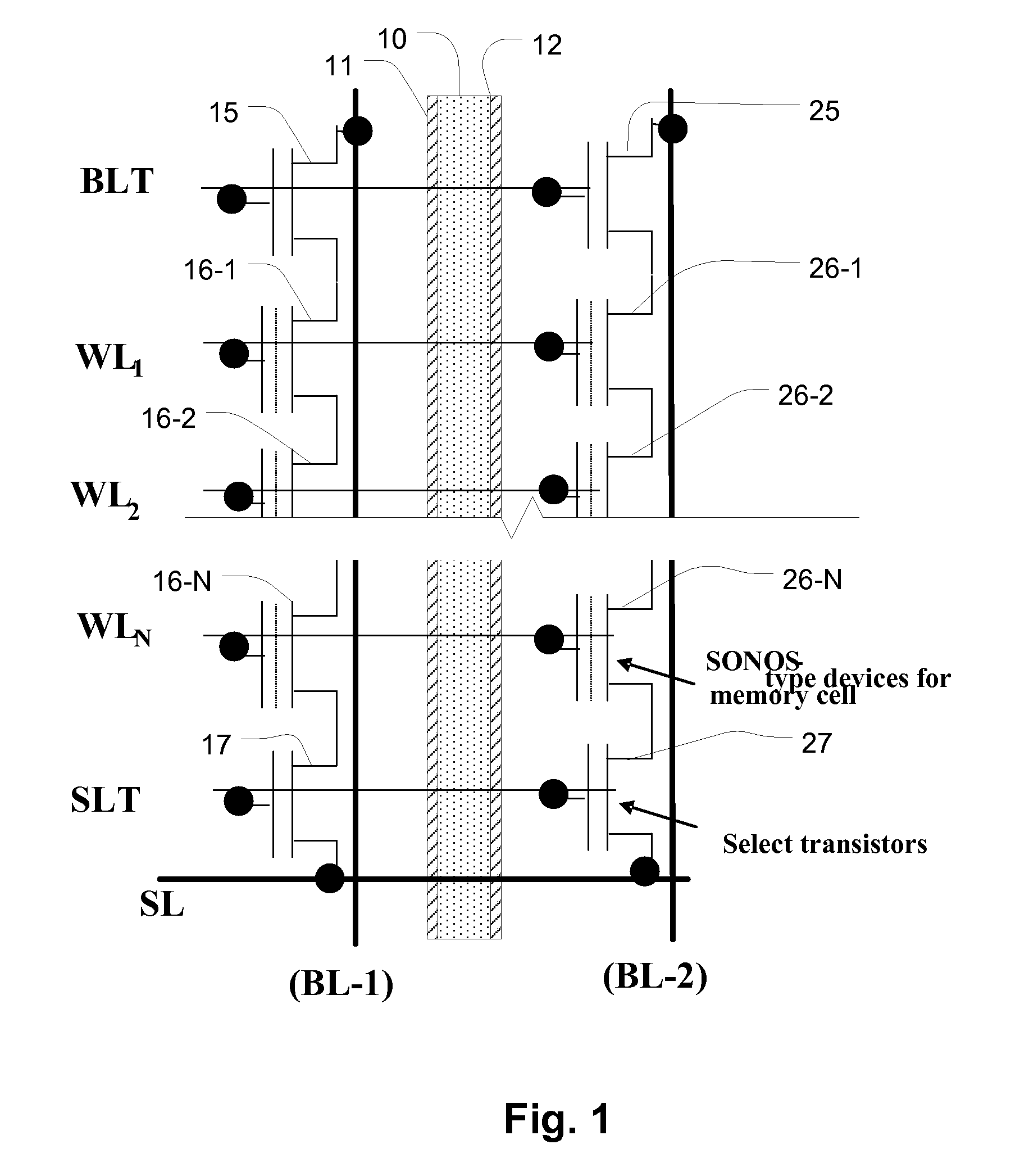
[0046]FIG. 1 is schematic illustration of a portion of a NAND array showing shallow trench isolation schematically in region 10 and lateral pocket implants in regions 11, 12 as described herein. Memory cells are arranged in a plurality of NAND strings, where a first NAND string in FIG. 1 includes memory cells 16-1 through 16-N connected in series and a second NAND string includes memory cells 26-1 through 26-N connected in series, where N may be 16 or 32 or higher. A corresponding set of word lines WL1 through WLN is coupled to respective memory cells within the NAND strings. A NAND string is selected by controlling the block transistors 15, 25 using the control line BLT to connect the series of memory cells to a bit line BL-1, BL-2, and source select transistors 17, 27 using the control line SLT to connect the series of memory cells to a reference line SL....


PUM


Abstract

A charge trapping memory cell is described, having pocket implants along the sides of the channel and having the same conductivity type as the channel, and which implants have a concentration of dopants higher than in the central region of the channel. This effectively disables the channel in the region of non-uniform charge trapping caused by a bird's beak or other anomaly in the charge trapping structure on the side of the channel. The pocket implant can be formed using a process compatible with standard shallow trench isolation processes.

Description

RELATED APPLICATIONS[0001]The benefit is claimed of U.S. Provisional Patent Application No. 60 / 954,819 filed 9 Aug. 2007; and of U.S. Provisional Patent Application No. 61 / 019,519 filed 7 Jan. 2008, both of which are incorporated by reference as if fully set forth herein.BACKGROUND OF THE INVENTION[0002]1. Field of the Invention[0003]The invention relates generally to nonvolatile memory devices, and in particular to flash memory cells and manufacturing of flash memory devices.[0004]2. Description of Related Art[0005]Flash memory technology includes memory cells that store charge between the channel and gate of a field effect transistor. The charge stored affects the threshold of the transistor, and the changes in threshold due to the stored charge can be sensed to indicate data.[0006]One type of charge storage memory cell in widespread application is known as a floating gate memory cell. In a floating gate memory cell, a floating gate of conductive material, such as a conductive pol...

Claims


Application Information

Patent Timeline
Patent Type & Authority Patents(United States)
IPC IPC(8): H01L29/792
CPCG11C11/5621G11C16/0466G11C16/0483G11C16/10H01L27/115H01L27/11568H01L29/4234H01L29/792H10B43/30H10B69/00
Inventor LUE, HANG-TING
Owner MACRONIX INT CO LTD
Why Eureka
Try Eureka