
Solid element device and method for manufacturing the same

a technology of solid elements and components, applied in glass reforming devices, glass making apparatus, manufacturing tools, etc., can solve problems such as yellowing and inability to provide sample devices by the continuation of resin sealing

Inactive Publication Date: 2010-11-02
TOYODA GOSEI CO LTD +1
View PDF92 Cites 50 Cited by
  • Summary
  • Abstract
  • Description
  • Claims
  • Application Information

AI Technical Summary

Benefits of technology

The invention provides a solid element device that includes a solid element, an electric power receiving and supplying part, and an inorganic sealing material for sealing the solid element. The device can also include a heat resistant member for covering the electrical connection part and a part of the electric power receiving and supplying part. The inorganic sealing material can be made of low melting glass selected from several options. The method of making the device involves mounting the solid element on the electric power receiving and supplying part and then pressing the inorganic sealing material in an oxygen barrier atmosphere at a temperature at or above the deformation point of the sealing material to perform sealing. The technical effects of the invention include improved reliability and durability of the solid element device, as well as improved sealing performance and protection of the electric power receiving and supplying part.

Problems solved by technology

In such solid element devices, it is known that, upon exposure to high intensity light, the light transparent resin causes deterioration such as yellowing.
According to the solid element devices using the conventional low melting glass as the sealing member, although the glass is low melting glass, high temperature fabrication should be carried out, and, due to the hard material, in fact, disadvantageously, any sample device cannot be provided by the continuation of the resin sealing.

Method used


Image

  • Solid element device and method for manufacturing the same
  • Solid element device and method for manufacturing the same
  • Solid element device and method for manufacturing the same

Examples


example 1

[0267]In this example, a face-up-type group III nitride-based compound semiconductor light emitting element 1010 shown in FIG. 30 was used as an optical element. This light emitting element emits blue light.

[0268]The specifications of each layer constituting the light emitting element 1010 are as follows.

[0269]

LayersCompositionp-type layer 1015p-GaN:MgLayer 1014 including lightIncluding InGaN layeremitting layern-type layer 1013n-GaN:SiBuffer layer 1012AlNSubstrate 1011Sapphire

[0270]The n-type layer 1013 made of GaN doped with Si as an n-type impurity is formed on the substrate 1011 through the buffer layer 1012. In this example, sapphire is used as the substrate 1011. The material for the substrate 1011, however, is not limited to sapphire, and examples of materials usable herein include sapphire, spinel, silicon carbide, zinc oxide, magnesium oxide, manganese oxide, zirconium boride, and group III nitride-based compound semiconductor single crystals. The buffer layer is formed by ...

example 2

[0282]An optical device 1003 shown in FIG. 34 has the same construction as the optical device 1001 shown in FIG. 33, except that the low melting glass contains a fluorescent material. In FIGS. 33 and 34, like parts are identified with the same reference numerals, and the explanation thereof will be omitted. In this example, the sealing member 1038 is made of low melting glass doped with a rare earth element as the fluorescent material.

[0283]The incorporation of an optional fluorescent material in the low melting glass can realize control of the color of light emitted from the optical device 1003.

example 3

[0284]An optical device 1004 shown in FIG. 35 has the same construction as the optical device 1002 shown in FIG. 4, except that the sealing member 1028 is covered by a shell-shaped cover 1048. This cover 1048 is made of an epoxy resin or other light transparent resin and is formed by molding. The provision of the cover 1048 can provide a large optical device. Thus, a wide variety of optical systems can be provided by preparing a glass sealing body having a standard shape and then using a resin for which equipment of mold and molding work are easier. In this case, the density of light emitted from the light emitting element is high, and a glass material is provided around the light emitting element which causes a temperature rise. Therefore, deterioration in the optical output can be suppressed to such a level that is negligible. The sealing member 1038 shown in FIG. 34 can also be covered by this cover 1048. Further, each of sealing members 1058, 1068, 1069, 1079 shown in FIGS. 36, ...


PUM

PropertyMeasurementUnit
viscosityaaaaaaaaaa
viscosityaaaaaaaaaa
melting pointaaaaaaaaaa

Abstract

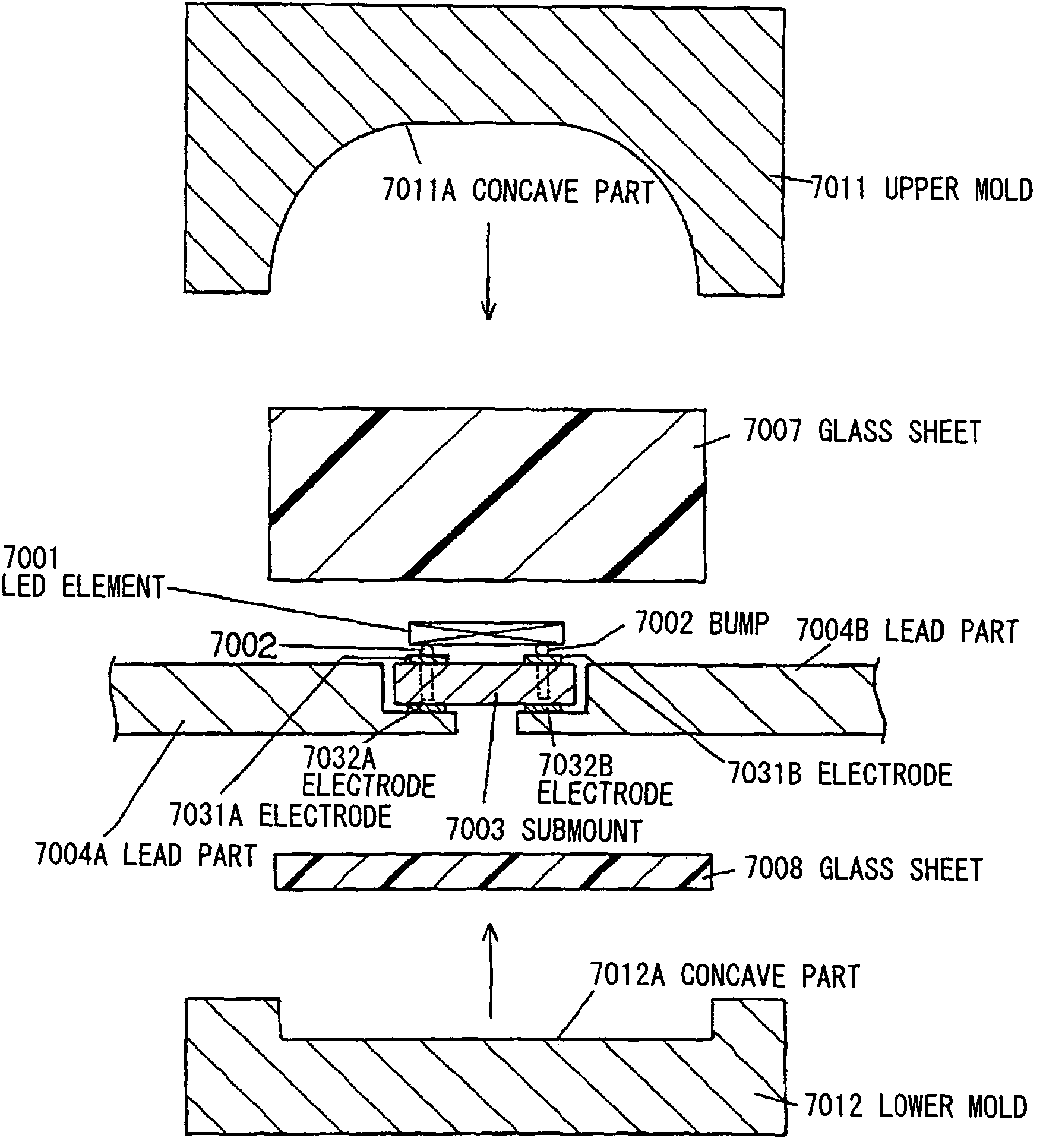
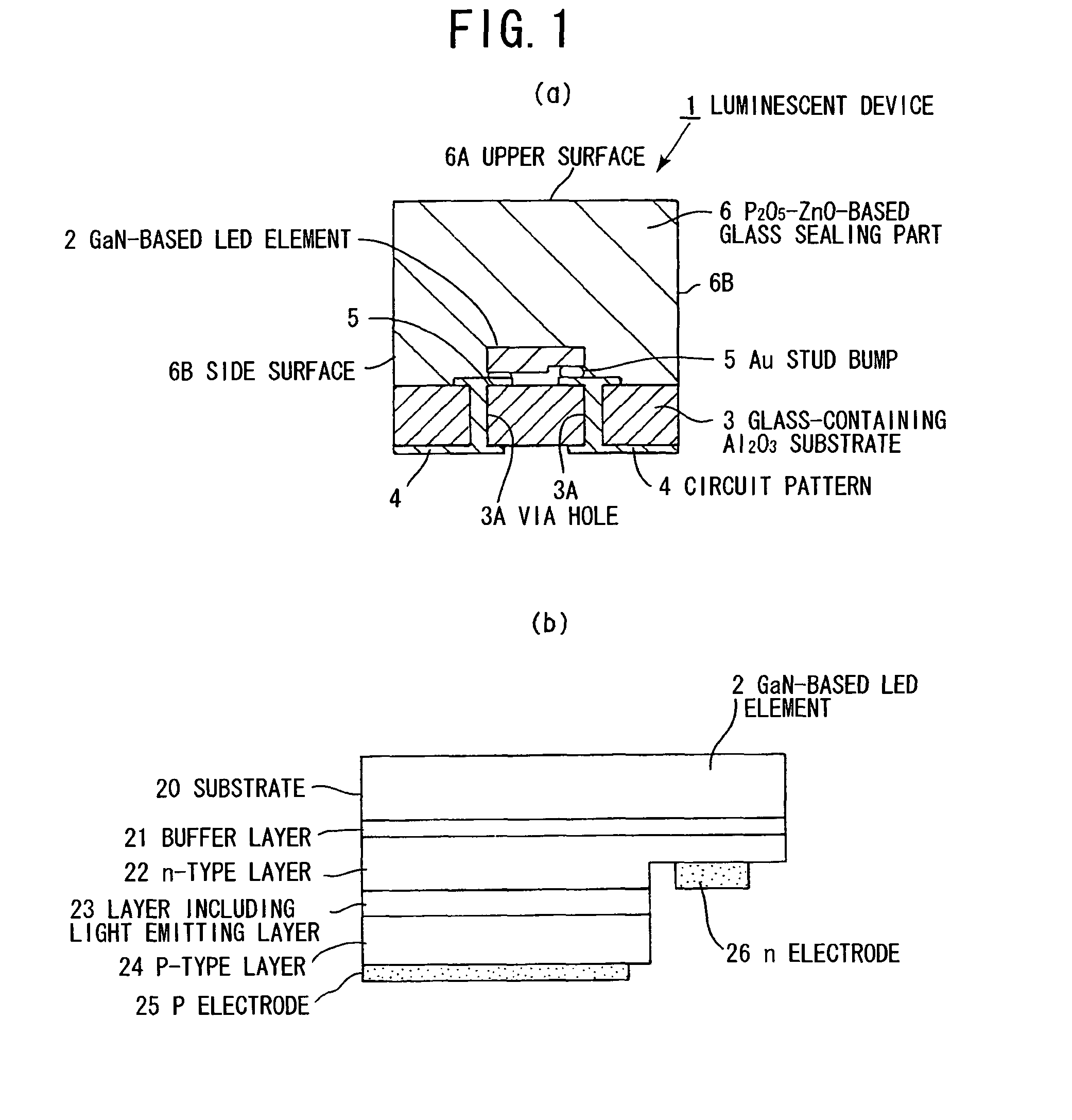
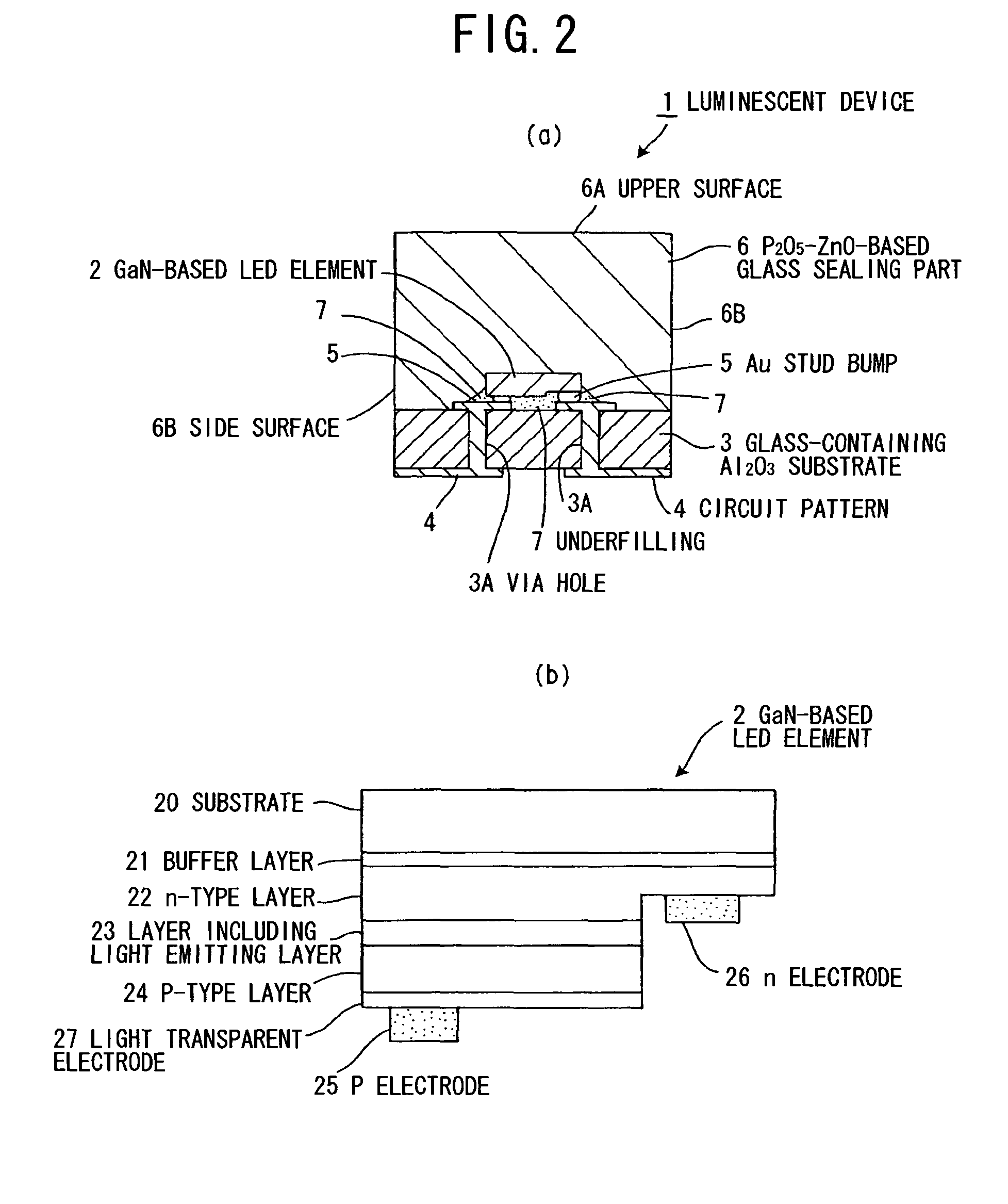
A method for manufacturing a solid element device, which comprises providing a glass-containing Al2O3 substrate (3) having a GaN based LED element (2) placed thereon, setting a P2O5—ZnO based low melting point glass in parallel with the substrate, and carrying out a press working at a temperature of 415° C. or higher under a pressure of 60 kgf in a nitrogen atmosphere. Under these conditions, the low melting point glass has a viscosity of 109 poise, and is adhered via an oxide formed on the surface of the glass-containing Al2O3 substrate (3). A solid element device manufactured by the above method can be manufactured through a glass sealing working at a low temperature and also has a highly reliable sealing structure.

Description

[0001]This application is based on Japanese Patent Application Nos. 2003-063015, 2003-160855, 2003-160867, 2003-193182, 2003-342705, 2003-342706, and 2004-010385, the entire disclosures of which are incorporated herein by reference.TECHNICAL FIELD[0002]The invention relates to a solid element device (or solid-state device) comprising an optical element sealed with a glass material, and particularly to a solid element device using a low melting glass material as a glass material.BACKGROUND ART[0003]Solid element devices comprising a solid element, such as a light emitting diode, sealed with a light transparent resin material such as an epoxy resin have hitherto been known. In such solid element devices, it is known that, upon exposure to high intensity light, the light transparent resin causes deterioration such as yellowing. In particular, when a group III nitride-based compound semiconductor light emitting element which emits short-wavelength light is used, the light transparent re...

Claims


Application Information

Patent Timeline
Patent Type & Authority Patents(United States)
IPC IPC(8): H01L21/56H01L33/48H01L33/56H01L33/62
CPCH01L33/56H01L24/17H01L2924/12041H01L2933/005H01L2924/01057H01L24/45H01L2224/48247H01L2924/3025H01L2224/92125H01L2224/73265H01L2224/73204H01L2224/48465H01L2224/48227H01L2224/48091H01L2224/32225H01L2224/16225H01L2924/01322H01L2224/45144H01L2924/00014H01L2924/00H01L2924/00012H01L2924/15787H01L2924/181H01L2924/12035H01L2924/12042H01L2924/12036H01L24/73H01L2224/48257H01L2224/97H01L2224/14H01L2224/48237C03B23/20C03C8/24C03C27/06H01L33/62
Inventor SUEHIRO, YOSHINOBUINOUE, MITSUHIROKATO, HIDEAKIHADAME, KUNIHIROTOHMON, RYOICHIWADA, SATOSHIOTA, KOICHIAIDA, KAZUYAWATANABE, HIROKIYAMAMOTO, YOSHINORIOHTSUKA, MASAAKISAWANOBORI, NARUHITO
Owner TOYODA GOSEI CO LTD
Learn More