Method for forming vias in a substrate
a technology of vias and substrates, applied in the direction of basic electric elements, electrical equipment, semiconductor/solid-state device manufacturing, etc., can solve the problem of uniform electric capacity
- Summary
- Abstract
- Description
- Claims
- Application Information
AI Technical Summary
Benefits of technology
Problems solved by technology
Method used
Image
Examples
first embodiment
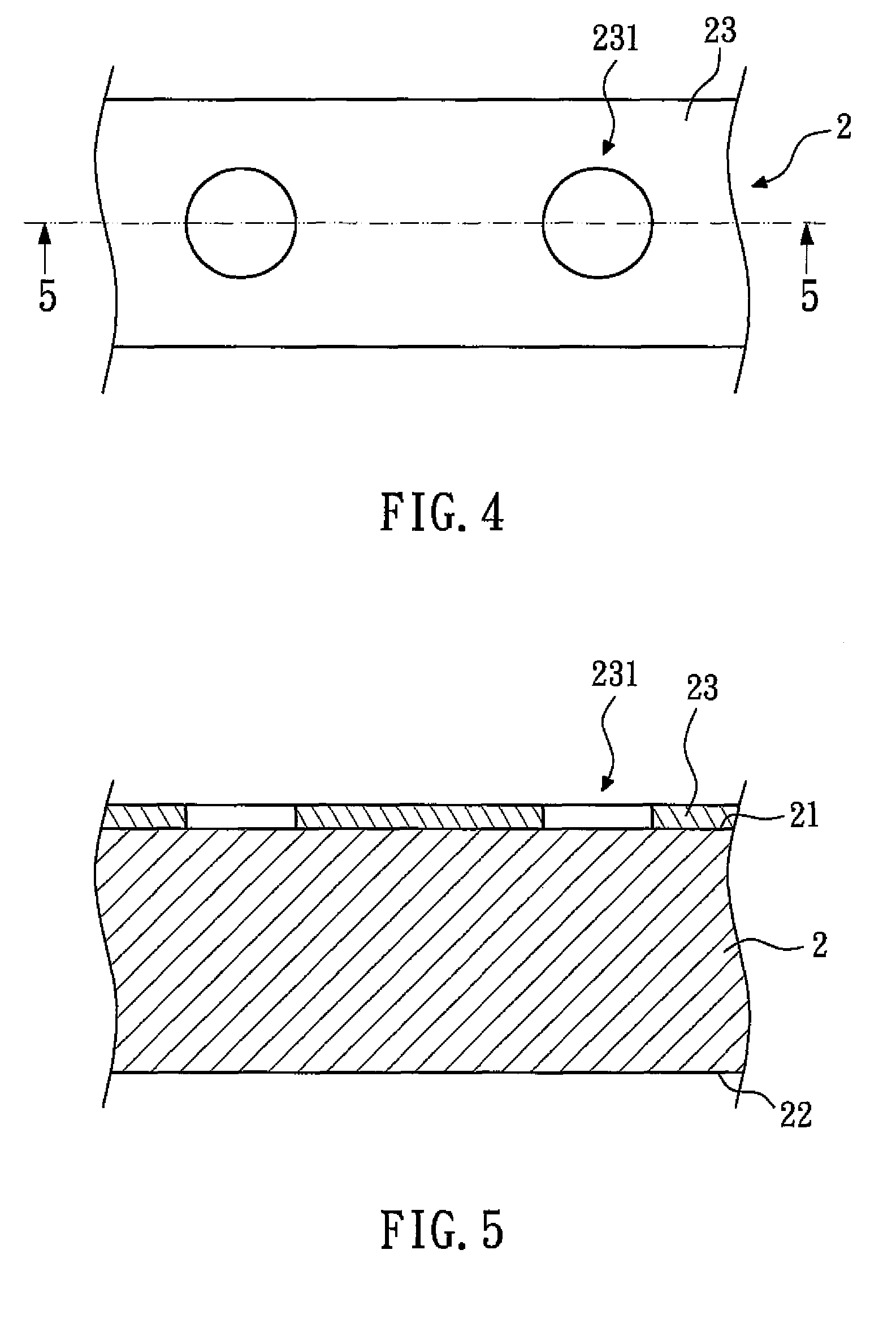
[0014]FIGS. 4 to 19 show the schematic views of the method for forming vias in a substrate according to the present invention. Referring to FIG. 4, a top view of the substrate 2, and FIG. 5, a cross-sectional view of the substrate 2 along line 5-5 in FIG. 4, first, a substrate 2 is provided. The substrate 2 has a first surface 21 and a second surface 22. The substrate 2 is, for example, a wafer or made from silicon. Afterward, a first photo resist layer 23 is formed on the first surface 21 of the substrate 2, and a first opening 231 is formed on the first photo resist layer 23. In the embodiment, the first opening 231 is circular from the top view. It is understood that the first opening 231 may be square from the top view.
[0015]Referring to FIG. 6, a groove 24 is formed on the substrate 2 according to the first opening 231 by etching or other methods, and the groove 24 does not penetrate the substrate 2. Afterward, the first photo resist layer 23 is removed. Then, referring to FIG....
second embodiment
[0023]FIGS. 20 to 27 show the schematic views of the method for forming vias in a substrate according to the present invention. Referring to FIG. 20, a top view of the substrate 4, and FIG. 21, a cross-sectional view of the substrate 4 along line 21-21 in FIG. 20, first, a substrate 4 is provided. The substrate 4 has a first surface 41 and a second surface 42. The substrate 4 is, for example, a wafer or made from silicon. Afterward, a first photo resist layer 43 is formed on the first surface 41 of the substrate 4, and a first opening 431 is formed on the first photo resist layer 43.
[0024]Referring to FIG. 22, a groove 44 is formed on the substrate 4 according to the first opening 431 by etching or other methods, and the groove 44 does not penetrate the substrate 4. Afterward, the first photo resist layer 43 is removed. Then, referring to FIG. 23, the groove 44 is filled with a conductive metal 45. In the embodiment, the material of the conductive metal 45 is copper, and the conduct...
PUM
| Property | Measurement | Unit |
|---|---|---|
| thickness | aaaaa | aaaaa |
| conductive | aaaaa | aaaaa |
| thickness | aaaaa | aaaaa |
Abstract
Description
Claims
Application Information
 - R&D
- Intellectual Property
- Life Sciences
- Materials
- Tech Scout
- Unparalleled Data Quality
- Higher Quality Content
- 60% Fewer Hallucinations
Browse by: Latest US Patents, China's latest patents, Technical Efficacy Thesaurus, Application Domain, Technology Topic, Popular Technical Reports.
© 2025 PatSnap. All rights reserved.Legal|Privacy policy|Modern Slavery Act Transparency Statement|Sitemap|About US| Contact US: help@patsnap.com


