
Method for eliminating negative slack in a netlist via transformation and slack categorization

a technology of netlist and negative slack, applied in the field can solve the problems of strategy having a significant adverse impact on the runtime, affecting the timing of vlsi chips, and affecting the placement and synthesis of vlsi chips, so as to efficiently improve the timing of vlsi chip design during placement and synthesis.

Active Publication Date: 2010-10-05
SIEMENS PROD LIFECYCLE MANAGEMENT SOFTWARE INC
View PDF17 Cites 5 Cited by
  • Summary
  • Abstract
  • Description
  • Claims
  • Application Information

AI Technical Summary

Benefits of technology

This patent describes a method and system for improving the timing of a VLSI chip design during placement and synthesis. The invention aims to efficiently address negative slack of particular synthesis or incremental placement transformations. It achieves this by dynamically adjusting slack targets and thresholds, reporting unfixable problems, and speeding up the process. The invention fundamentally changes the overall result by analyzing slack feasibility at each point in the flow and dynamically setting slack thresholds and targets to values that can physically be implemented. It also provides early insights into the design through the analysis of slack feasibility and guides the next flow step. The invention optimizes a design represented by a netlist in a single state of static timing analysis and dynamically eliminates a maximum negative slack. Overall, the invention improves the speed and quality of the chip design process.

Problems solved by technology

Furthermore, the flow sets a target slack thereof.
This strategy may have a significant adverse impact on the runtime.(g) How does the optimization flow determine which is a failing slack in the design.
However, the manner of how the gates and nets are connected between the latches (timing paths) is critical.
Prior art systems designed as described previously present a number of drawbacks:(a) The slack threshold to select portions of the design to optimize is constant (usually set to zero slack).
This is an impossible situation for which no transformation to the circuit topology or structure can eliminate the negative timing slack; and 2) the negative slack on a particular path under consideration may be dominated by elements which cannot be transformed through available transformations in a particular step.
For example, if a circuit path includes an SRAM, there are no transformations during the synthesis step 104 that can improve the circuit performance.ii) The particular transformation applied to individual gates in a given step may not be able to completely eliminate the negative slack on the path even when applied to the entire path.
For instance, the circuits on the path may be underpowered or under-buffered, i.e., purely structural transformations will be unable to eliminate the negative slack because the required transformation will not be performed.
No structural or topological transformations will be able to eliminate the negative slack from this path.
An inefficient logic structure exists that prevents the negative slack from being eliminated by repowering, buffering, or location altering transformation.
This inevitably leads to time being wasted by applying transformations that do not work to achieve the goal of eliminating negative slack from the design.ii) The best transformation for eliminating negative slack in a particular instance is not necessarily the first one to be applied, leading to an inefficient structural implementation of the desired logical functionality.
While buffering improves but does not eliminate the negative slack, the presence of buffers limits whatever the replacement transforms can achieve.
This reset is based on accounting rather than on a specific knowledge about the state of the netlist.(d) The net effect of the existing process resides in that both time and effort are wasted and the final circuit implementation is less effective because optimizations do not assess their capabilities with respect to an encompassing flow, and maintain the underlying bad assumption that all the paths can achieve a unique slack target.
It cannot assess the amount of timing closure that the individual optimization transforms require.
Further, it cannot tell the optimization tool when to stop attempting to buffer or repower the design.
Extending this concept to timing without actually applying the transform is difficult, and therefore it negates the timing closure problem.
This approach does not answer the problem of which transforms to be applied and when to stop.
U.S. Patent Application No. 2006 / 0015836, published Jan. 19, 2006, describes a comparison between two different domains as a means of weighting nets for placement, but does not address optimization.

Method used


Image

  • Method for eliminating negative slack in a netlist via transformation and slack categorization
  • Method for eliminating negative slack in a netlist via transformation and slack categorization
  • Method for eliminating negative slack in a netlist via transformation and slack categorization

Examples


example

[0075]Referring to FIG. 4, there is shown an exemplary implementation corresponding to the preferred embodiment. The technique is not limited to the timing environments or transformations to be illustrated hereinafter. The design is first loaded and timing assertions are applied. For the purposes of the illustrative example, it will be assumed that all transformations belong to a single category.

[0076]In the initial step, the contrived timing environment is setup (step 401) with all the gates and wires having zero delay and all the pin capacitances being forced to zero. This environment is designed to expose slack failures that are caused by timing assertions since no other netlist elements will contribute to the circuit delay. Timing analysis is run on the design to obtain the list of slacks at each timing point. This list is referred to as the ZOPTog list. The list of negative slacks ZOPTog is reported to the user so that timing assertion adjustments can be made. This information ...


PUM


Abstract

A method for eliminating negative slack in a netlist representing a chip design uses a contrived timing environment to overlay information onto the design environment during logic and physical synthesis phase. The overlaid timing information determines which netlist transformation provides a maximum leverage for the negative slack elimination and a way for creating a dynamic transformation recipe tuned for each design. The method further provides upper bounds on the negative slack elimination to prevent the netlist transforms from being applied to situations exceeding the capabilities for improving the design.

Description

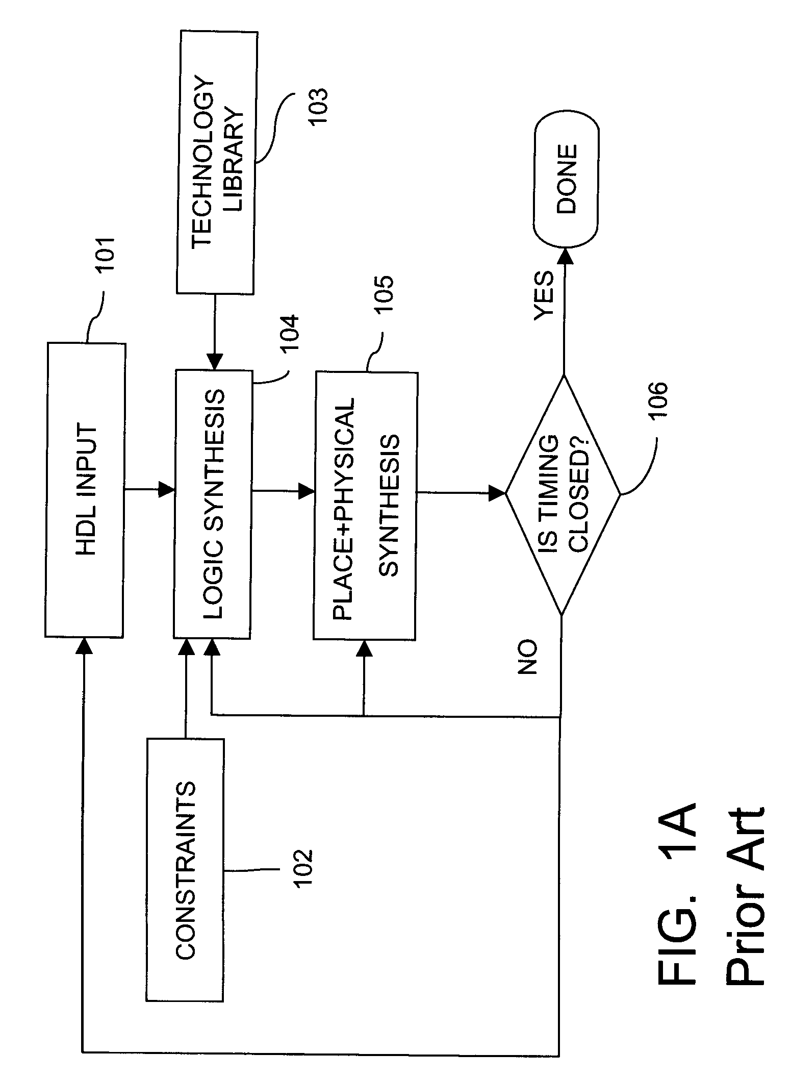
FIELD OF THE INVENTION[0001]This invention relates to the electronic design of Very Large Scale Integrated (VLSI) chips, and more particularly, to a method of eliminating negative timing slack in the chip to guarantee proper functionality.RELATED PRIOR ART[0002]The design of VLSI circuits has witnessed an unprecedented growth in the number and complexity of digital circuits. As a result, designers have adapted to this environment by using higher levels of abstraction in their designs, some of which have become proficient in managing the complexity of the design by developing new design languages and tools.[0003]Referring to FIG. 1a, there is shown a prior art flowchart illustrating the design of a VLSI chip beginning with a high-level description language (HDL) through the physical synthesis phase. The designer describes the functionality of the chip, preferably using HDL (step 101) as the input language or, alternatively, Verilog or VHDL (Very High Speed HDL). Further described are...

Claims


Application Information

Patent Timeline
Patent Type & Authority Patents(United States)
IPC IPC(8): G06F17/50
CPCG06F17/5031G06F17/5045G06F2217/84G06F30/3312G06F2119/12G06F30/30G06F30/3315
Inventor CURTIN, JAMES J.DOUGHERTY, JR., WILLIAM E.NEVES, JOSE L.SEARCH, DOUGLAS S.
Owner SIEMENS PROD LIFECYCLE MANAGEMENT SOFTWARE INC
Learn More