
Symmetrically and asymmetrically stacked transistor group RF switch

a transistor group and stacked technology, applied in the field of switches, can solve the problems of first type of compression, undesirable input signal feedthrough, loss of power, etc., and achieve the effect of improving rf switch design, vastly reducing the ic area required for rf switch implementation, and high area efficiency

Inactive Publication Date: 2010-09-14
PSEMI CORP
View PDF41 Cites 323 Cited by
  • Summary
  • Abstract
  • Description
  • Claims
  • Application Information

AI Technical Summary

Benefits of technology

The RF switch design achieves reduced insertion loss, improved isolation, and increased 1 dB compression point, enabling efficient high-frequency operation with reduced manufacturing costs and enhanced integration capabilities.

Problems solved by technology

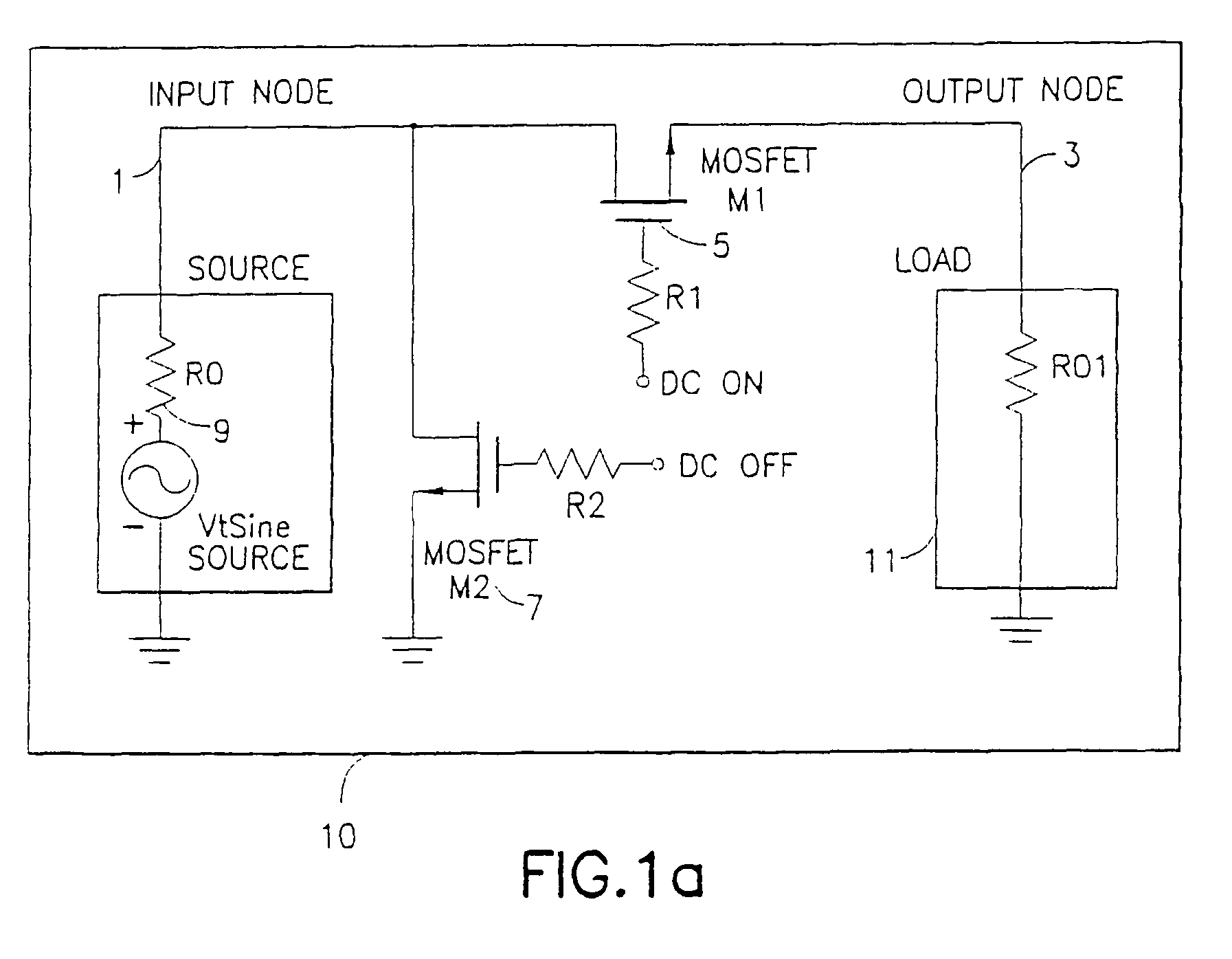
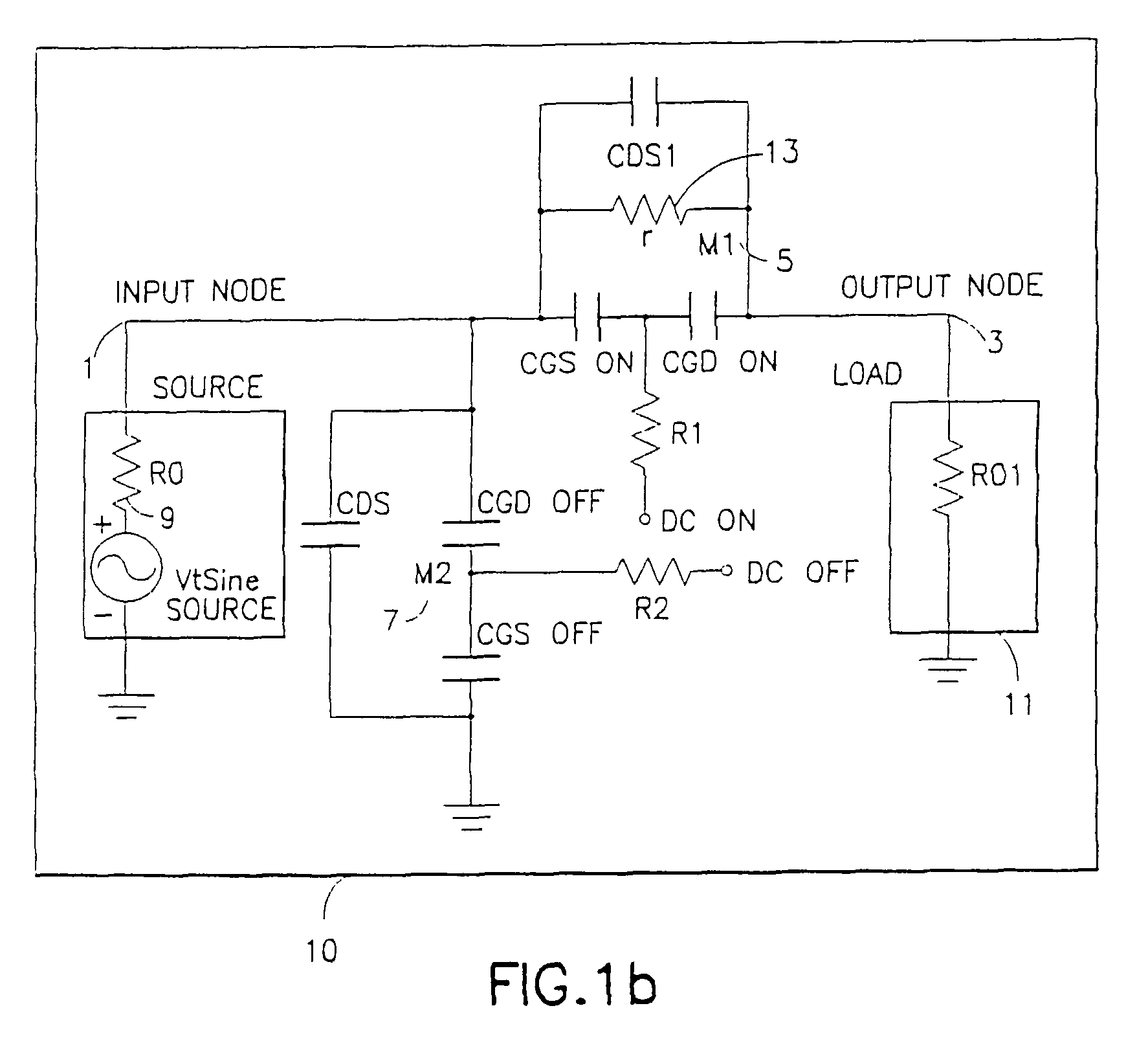
Feedthrough of the input signal is undesirable and is directly related to the input-to-output isolation of the RF switch 10.
This loss of power increases for increased input power (i.e., input signals of increased power), and thereby causes a first type of compression.
At breakdown, the shunt device begins to heavily conduct current thereby reducing the power available at the output.
The prior art RF switch implementations attempt to improve the RF switch performance characteristics described above, however, they do so with mixed results and with varying degrees of integrated circuit complexity and yields.
For example, bulk CMOS RF switches disadvantageously exhibit high insertion loss, low compression, and poor linearity performance characteristics.
For example, GaAs technology exhibits relatively low yields of properly functioning integrated circuits.
GaAs RF switches tend to be relatively expensive to design and manufacture.
In addition, although GaAs switches exhibit improved insertion loss characteristics as described above, they may have low frequency limitations due to slow states present in the GaAs substrate.
The technology also does not lend itself to high levels of integration, which requires that digital control circuitry associated with the RF switch be implemented “off chip” from the switch.
The low power control circuitry associated with the switch has proven difficult to integrate.
This is disadvantageous as it both increases the overall system cost or manufacture, size and complexity, as well as reducing system throughput speeds.
Such integration has been heretofore difficult to achieve using Si and GaAs substrates.

Method used


Image

  • Symmetrically and asymmetrically stacked transistor group RF switch
  • Symmetrically and asymmetrically stacked transistor group RF switch
  • Symmetrically and asymmetrically stacked transistor group RF switch

Examples


first embodiment

Negative Voltage Generator-Charge Pump—A First Embodiment

[0079]As shown in FIG. 4, one embodiment of the fully integrated RF switch 100 includes a negative voltage generator or charge pump 120. The negative voltage generator 120 generates the negative power supply voltage (specified hereafter as “−Vdd”) required by other circuits of the fully integrated RF switch 100. Two sets of inputs are provided to the negative voltage generator 120: a positive DC power supply voltage signal (Vdd) 122; and a clocking input (shown in the figure as a single input signal, “Clk”) 124. Although the clocking input 124 is shown as a single input signal in FIG. 4, as described below with reference to FIG. 5b, in some embodiments of the present inventive RF switch, the clocking input 124 may comprise two or more clock input signals.

[0080]In addition, in the embodiment shown in FIG. 4, the positive supply voltage that is input to the negative voltage generator circuit 120 comprises a 3 VDC power supply. H...


PUM


Abstract

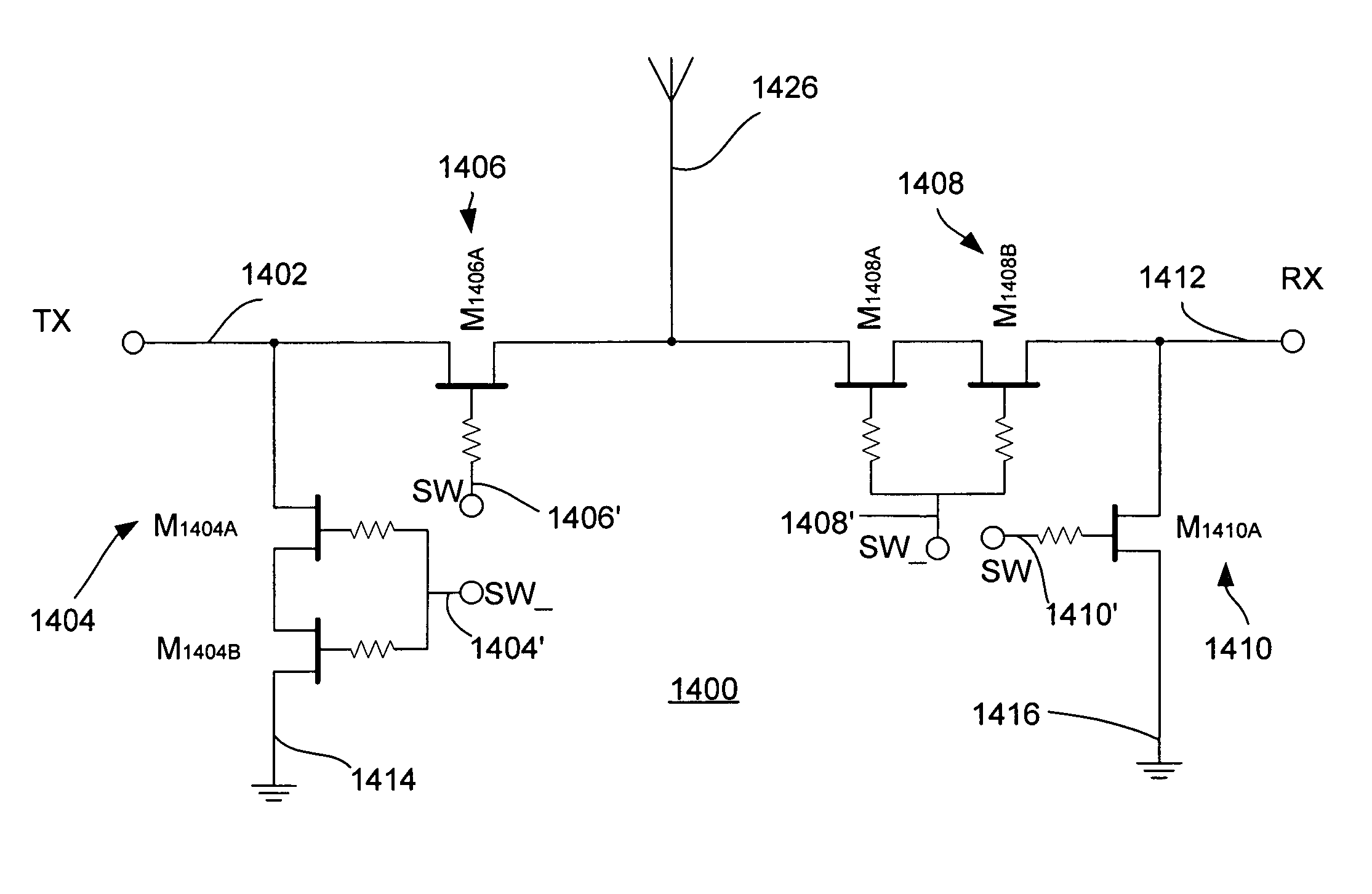
A silicon-on-insulator (SOI) RF switch adapted for improved power handling capability using a reduced number of transistors is described. In one embodiment, an RF switch includes pairs of switching and shunting stacked transistor groupings to selectively couple RF signals between a plurality of input / output nodes and a common RF node. The switching and shunting stacked transistor groupings comprise one or more MOSFET transistors connected together in a “stacked” or serial configuration. In one embodiment, the transistor groupings are “symmetrically” stacked in the RF switch (i.e., the transistor groupings all comprise an identical number of transistors). In another embodiment, the transistor groupings are “asymmetrically” stacked in the RF switch (i.e., at least one transistor grouping comprises a number of transistors that is unequal to the number of transistors comprising at least one other transistor grouping). The stacked configuration of the transistor groupings enable the RF switch to withstand RF signals of varying and increased power levels. The asymmetrically stacked transistor grouping RF switch facilitates area-efficient implementation of the RF switch in an integrated circuit. Maximum input and output signal power levels can be withstood using a reduced number of stacked transistors.

Description

[0001]This application is a Continuation-in-Part (CIP) of commonly assigned U.S. patent application Ser. No. 10 / 922,135, filed Aug. 18, 2004 now U.S. Pat. No. 7,123,898, entitled “Switch Circuit and Method of Switching Radio Frequency Signals”, which is a continuation of U.S. Pat. No. 6,804,502 issued Oct. 12, 2004, entitled “Switch Circuit and Method of Switching Radio Frequency Signals”, filed on Oct. 8, 2002 as application Ser. No. 10 / 267,531, which claims the benefit under 35 U.S.C. §119 (e) of U.S. Provisional Application No. 60 / 328,353, filed Oct. 10, 2001, entitled “Silicon-on-Insulator RF Switches”; this application also claims the benefit under 35 U.S.C. §119 (e) of U.S. Provisional Application No. 60 / 650,033, filed Feb. 3, 2005, entitled “Symmetrically and Asymmetrically Stacked Transistor Grouping RF Switch”; and the contents of application Ser. No. 10 / 922,135, U.S. Pat. No. 6,804,502, its related provisional application (U.S. Provisional Application No. 60 / 328,353), and ...

Claims


Application Information

Patent Timeline
Patent Type & Authority Patents(United States)
IPC IPC(8): H04B1/24H04M1/00H01L29/76
CPCH03K17/063H03K17/6871H03K17/693H02M3/073
Inventor KELLY, DYLAN J.BURGENER, MARK L.
Owner PSEMI CORP
Learn More