Wafer level chip size package for MEMS devices and method for fabricating the same
a technology of mems devices and wafers, applied in the field of wafer level chip size packages, can solve the problems of affecting the quality of wafers, and affecting the quality of wafers, and achieve the effect of improving the wafer level chip size packag
- Summary
- Abstract
- Description
- Claims
- Application Information
AI Technical Summary
Benefits of technology
Problems solved by technology
Method used
Image
Examples
embodiment 1
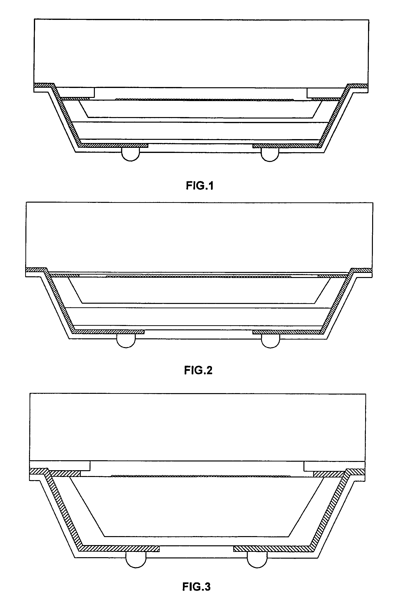
[0067]As shown in FIG. 14, of the present invention, a wafer level chip size package for MEMS devices includes a substrate wafer 20, a cap substrate 5, a cushion layer 25, a layer of redistribution leads 30, solder mask 35 and a plurality of solder bumps 40.
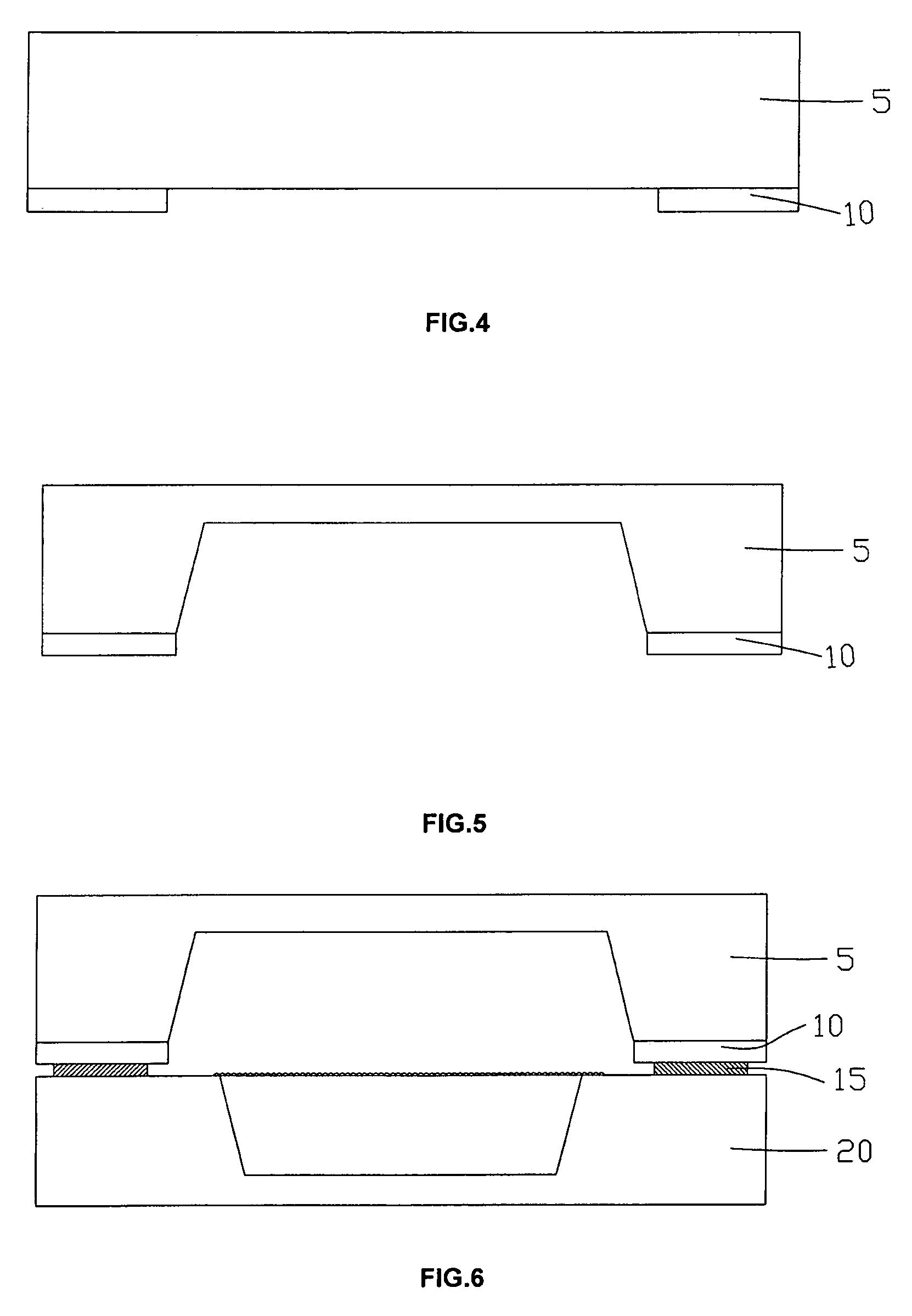
[0068]The substrate wafer 20 has formed thereon MEMS dies formed with certain MEMS structures, such as gears, hinges, slides, etc. There are also electrical terminals, preferably in the form of so called compatible pads 15 disposed at the periphery of each of the MEMS dies on the substrate wafer 20.
[0069]The cap substrate 5 has cavities which can be filled in inert gas with a certain pressure. The cap substrate 5 includes cavity walls 10 by which the cap substrate 5 is combined with the substrate wafer 20, each of the MEMS dies being encased within a corresponding cavity. Preferably though not necessarily, the depth of cavities is within the approximate range of 300-400 um, the thickness of cavity walls 10 is within the approxim...
embodiment 2
[0089] of the present invention, instead of the steps illustrated in FIG. 4 and FIG. 5, an alternative method of forming the cavity walls 10 is illustrated from FIG. 15 to FIG. 18.
[0090]As illustrated in FIG. 15, deposit a passivation layer 45 on the front side of the cap substrate 5 by PECVD (plasma enhanced chemical vapor deposition), spin coat photo resist 50 on the passivation layer 45, make pattern by lithography, the area which need not to be etched should be covered by photo resist 50.
[0091]As illustrated in FIG. 16, plasma etch at the front side of the cap substrate, the photo resist 50 will protect the passivation layer 45 from being etched while the exposed passivation layer 45 will be etched. After etching, strip the photo resist 50, the pattern of the passivation layer 45 is the same as that of the photo resist 50.
[0092]As illustrated in FIG. 17, make cavities on the cap substrate 5 by wet etching or dry etching, utilize the passivation layer 45 as a mask so that the pos...
PUM
 Abstract
Description
Claims
Application Information
 - R&D
- Intellectual Property
- Life Sciences
- Materials
- Tech Scout
- Unparalleled Data Quality
- Higher Quality Content
- 60% Fewer Hallucinations
Browse by: Latest US Patents, China's latest patents, Technical Efficacy Thesaurus, Application Domain, Technology Topic, Popular Technical Reports.
© 2025 PatSnap. All rights reserved.Legal|Privacy policy|Modern Slavery Act Transparency Statement|Sitemap|About US| Contact US: help@patsnap.com


