High frequency power amplifier
a power amplifier and high frequency technology, applied in the direction of amplifiers with semiconductor devices only, amplifiers with min 3 electrodes or 2 pn junctions, etc., can solve problems such as complicated switching control, and achieve the effect of high performance power and small footprin
- Summary
- Abstract
- Description
- Claims
- Application Information
AI Technical Summary
Benefits of technology
Problems solved by technology
Method used
Image

Examples
first embodiment
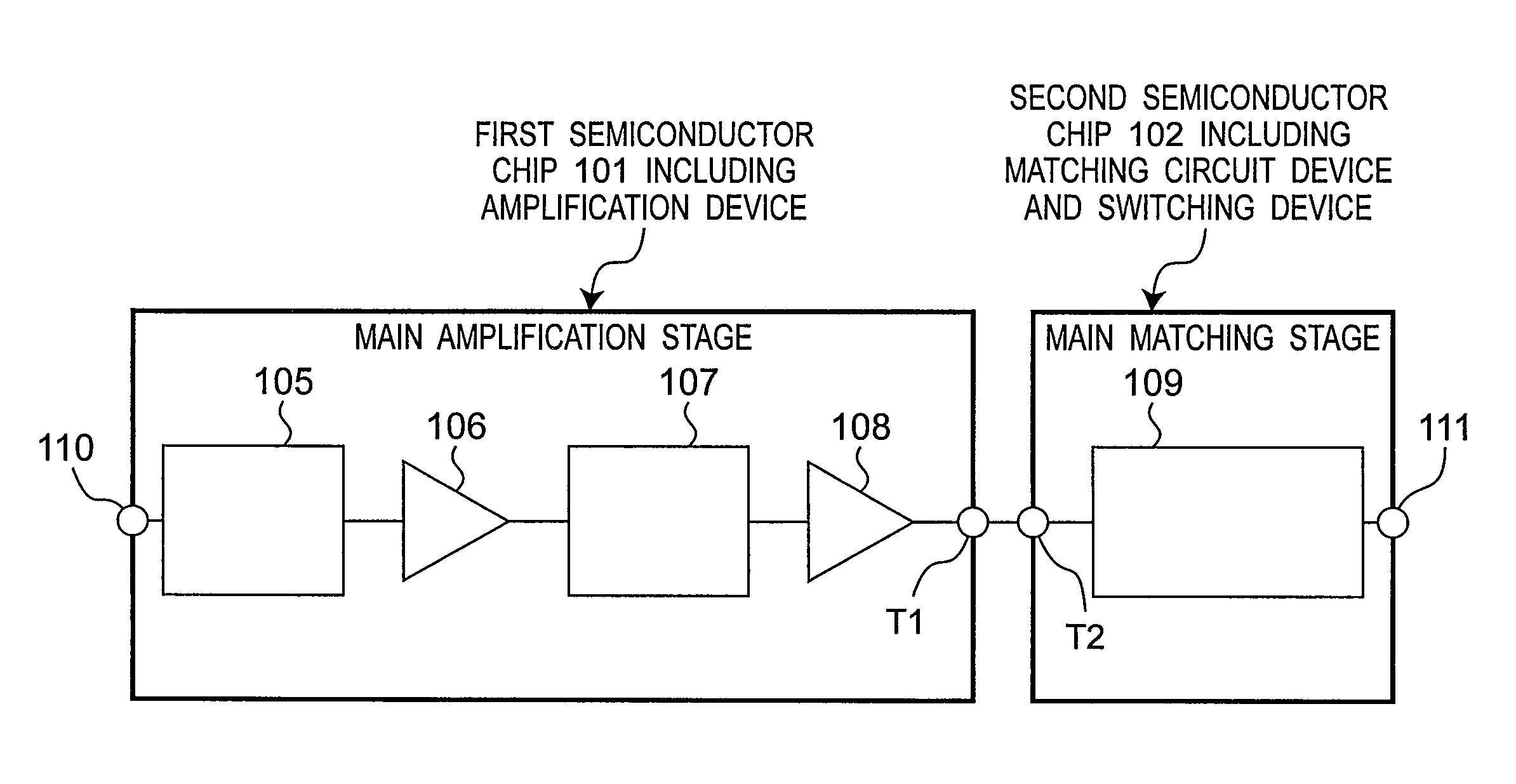
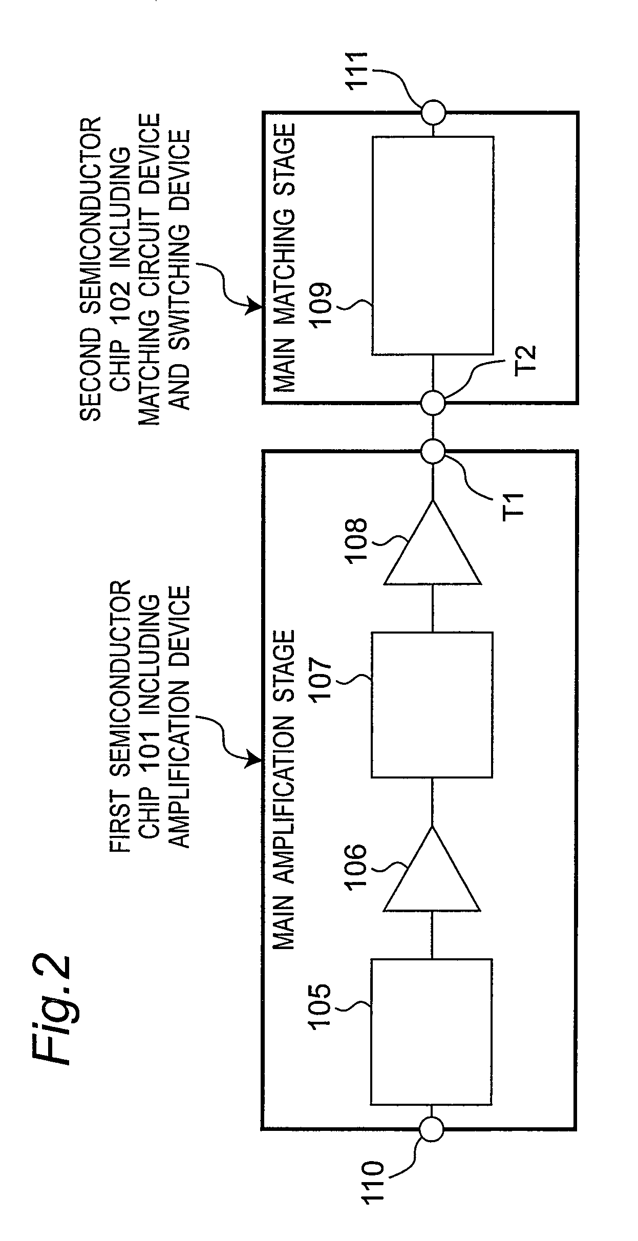
[0081]FIG. 6A is a circuit diagram corresponding to the arrangement shown in FIG. 2, and shows a first embodiment of a high frequency power amplifier employing the present invention.
[0082]This arrangement differs from the circuit shown in FIG. 5 in that a capacitor C11 and a switching device SW1 are added to the output matching circuit 109. Because the switching device SW1 is open when off and the capacitor C11 is not connected to the matching circuit as a ground capacitance, the output matching circuit state is equivalent to FIG. 5. When the switching device SW1 is on, the capacitor C11 is connected to the matching circuit as a ground capacitance, and the impedance of the matching circuit differs by the capacitance of C11 from the circuit shown in FIG. 5. The matching state of the output pin of the second amplification device therefore changes, efficiency can be optimized at two different output power levels or efficiency can be optimized at two different frequencies.
[0083]The outp...
second embodiment
[0105]An embodiment of a switching circuit that uses the switching device and matching circuit device formed on the second semiconductor chip is described next.
[0106]FIG. 10A, FIG. 10B, and FIG. 10C are circuit block diagrams describing a second embodiment of an impedance switching circuit according to the present invention. Reference numerals 215, 217, 218, 220, and 221 are capacitance devices, and reference numerals 216, 219, and 222 are switching devices. Referring to FIG. 10A, for example, when switching device 216 is on, the capacitance device 215 is connected to the circuit as a capacitance to ground, and when the switching device 216 is off, the to-ground side of the capacitance device 215 is open and the capacitance device 215 is not connected to the circuit. Because of the parasitic capacitance of an HEMT or other switching device, the capacitance to ground is the combined serial capacitance of the capacitance device 215 and the parasitic capacitance, but because this combi...
third embodiment
[0112]Another embodiment of a switching circuit is described below using FIG. 13A and FIG. 13B. The capacitances 237, 239, 241, 243 that are the matching devices are part of the matching circuit of the corresponding amplifier device, and the matching circuit is connected or disconnected by switching the control voltage (A) to (D) of the switching devices 238, 240, 242, 244 low (L) or high (H). Because there are four switches, a logic circuit 245 is provided and two control pins are used to switch the four control voltages (A) to (D) low or high. The four switching states are shown in FIG. 13B. This logic circuit is rendered on the second semiconductor chip in this embodiment of the invention, thus enabling controlling switching the impedance between more levels easily with a simple interface while reducing the chip size and the size of the amplifier device. Furthermore, because the logic circuit can be easily rendered using HEMT devices, for example, this function can be rendered on...
PUM
 Abstract
Description
Claims
Application Information
 - R&D
- Intellectual Property
- Life Sciences
- Materials
- Tech Scout
- Unparalleled Data Quality
- Higher Quality Content
- 60% Fewer Hallucinations
Browse by: Latest US Patents, China's latest patents, Technical Efficacy Thesaurus, Application Domain, Technology Topic, Popular Technical Reports.
© 2025 PatSnap. All rights reserved.Legal|Privacy policy|Modern Slavery Act Transparency Statement|Sitemap|About US| Contact US: help@patsnap.com