
Method for forming surface strap

a surface strap and conductive technology, applied in the direction of semiconductor devices, electrical equipment, transistors, etc., can solve the problems of complex method for forming a single buried strap at the collar of the trench capacitor in the trench capacitor dram structure, and the electric resistance of the buried strap to dramatically increase, so as to achieve the effect of simplifying the process and substantially lowering the electric resistance between the drain and the deep trench capacitor

Active Publication Date: 2009-07-07
NAN YA TECH
View PDF8 Cites 0 Cited by
  • Summary
  • Abstract
  • Description
  • Claims
  • Application Information

AI Technical Summary

Benefits of technology

This method effectively reduces electric resistance between the drain and deep trench capacitor, simplifies the process by intervening between deep trench capacitor and gate procedures, and allows for a larger contact area, mitigating the negative influence of strong electric fields on device performance.

Problems solved by technology

However, in addition to the fact that it is well known that it is not an optimal solution since it is very complicated and difficult to set the gate channel region in a gate trench of high aspect ratio plus the difficulty to control such device, high integration, shrinkage of the dimension of the capacitor as well as the shorter and shorter distance of the neighboring elements all cause the electric resistance of the buried strap to dramatically increase.
Besides, the method for forming the conventional single buried strap at the collar of the trench capacitor in the trench capacitor DRAM structure is complicated and needs improving.

Method used


Image

  • Method for forming surface strap
  • Method for forming surface strap
  • Method for forming surface strap

Examples


Embodiment Construction

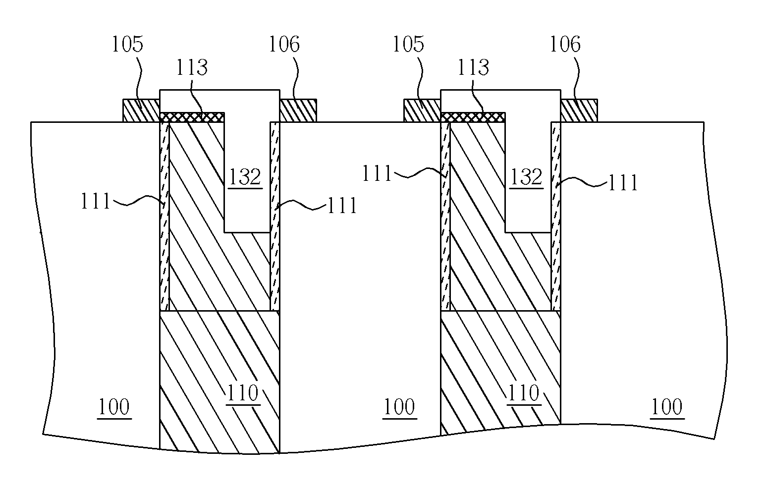
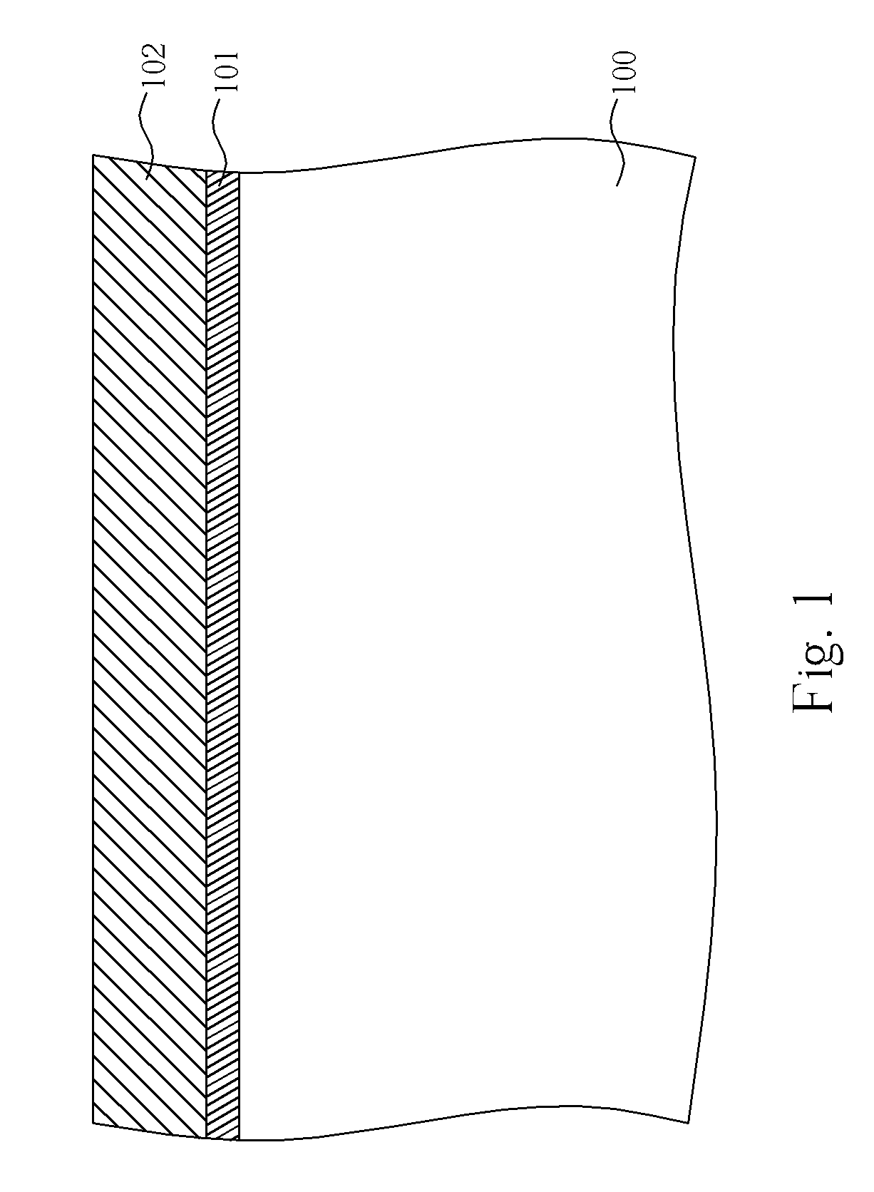
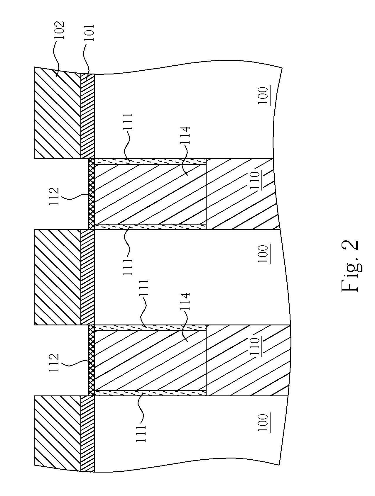
[0013]The present invention discloses a method for forming the surface strap characterized in that the surface strap connecting the capacitor to the drain is formed on the substrate rather than in the substrate. This method can effectively solve the problem that the strong electric field in the vicinity of the buried strap has negative influence on the performance of the devices. Second the method of the present invention intervening between the procedure of the deep trench capacitor and the procedure of the gate and may accordingly act as the hard mask of the procedure of the deep trench capacitor. Moreover performing the procedure of the surface strap before the procedure of the gate may simplify the process. Furthermore, if the conductive strap is made of a material with conductivity better than poly-Si, the electric resistance between the drain and the deep trench capacitor may be substantially lowered.

[0014]FIG. 1 to FIG. 9 illustrate the method for forming the surface strap of...


PUM


Abstract

A method for forming a surface strap includes forming a deep trench capacitor having a conductive connection layer on its surface in the substrate and the conductive connection layer in contact with the conductive layer; forming a poly-Si layer covering the pad layer and the conductive connection layer; performing a selective ion implantation with an angle to make part of the poly-Si layer an undoped poly-Si layer; removing the undoped poly-Si layer to expose part of the conductive connection layer; etching the exposed conductive connection layer to form a recess; removing the poly-Si layer to make the exposed conductive connection layer a conductive connection strap; filling the recess with an insulation material to form a shallow trench isolation; exposing the conductive layer; and selectively removing the conductive layer to form a first conductive strap which forms the surface strap together with the conductive connection strap.

Description

BACKGROUND OF THE INVENTION [0001]1. Field of the Invention[0002]The present invention relates to a method for forming a conductive strap. In particular, the present invention relates to a method for forming a conductive strap on the surface of a substrate.[0003]2. Description of the Prior Art[0004]A DRAM unit is made of a metal oxide semiconductor (MOS) transistor in series connection with a capacitor. In the current DRAM process, the capacitor is designed to be a stack capacitor on the surface of the substrate or a deep trench capacitor buried in the substrate.[0005]Because the deep trench capacitor is deeply buried in the substrate, conventionally a buried strap is used to electrically connect the drain and the deep trench capacitor in the MOS. However, in order to avoid the strong electric field caused by the drain and the buried strap as the electrical connection in the MOS to damage the performance of the devices, such as the raise of the dark current, the gate channel region ...

Claims


Application Information

Patent Timeline
Patent Type & Authority Patents(United States)
IPC IPC(8): H01L27/108H10B12/00
CPCH01L27/10867H10B12/0385
Inventor CHENG, CHIH-HAOLEE, TZUNG-HANLEE, CHUNG-YUAN
Owner NAN YA TECH
Learn More