
Low jitter and/or fast lock-in clock recovery circuit

a clock recovery and low jitter technology, applied in the direction of digital transmission, pulse automatic control, phase difference detection angle demodulation, etc., can solve the problems of high clock recovery difficulty, conventional pll jitter, and pll to have a very slow response time to any real change of data channel frequency, etc., to achieve fast lock-in time and high bandwidth

Inactive Publication Date: 2009-06-09
AVAGO TECH WIRELESS IP SINGAPORE PTE
View PDF6 Cites 1 Cited by
  • Summary
  • Abstract
  • Description
  • Claims
  • Application Information

AI Technical Summary

Benefits of technology

"The present invention is about a new apparatus that includes an oscillator circuit, a control circuit, a counter circuit, and a detector circuit. This apparatus can generate an output signal that oscillates at a particular frequency based on a control signal. The control circuit can generate the control signal based on a first error signal and a second error signal. The counter circuit can generate the first error signal based on the output signal and an input signal. The detector circuit can generate the second error signal based on the output signal and the input signal. The technical effects of this invention include providing a low jitter recovered channel clock, fast lock-in time, high bandwidth, and the ability to be implemented without high precision components. It can also be used in an optical data storage system and can be implemented without a slicer. The apparatus can intelligently turn on / off phase error gain and has separate programmable frequency error gain for error at maximum pulse width and for error at minimum pulse width, which is important to lower the jitter of the overall system."

Problems solved by technology

Such an implementation makes clock recovery more challenging since the recovered channel clock needs to have very low jitter in order to sample the data channel amplitude at a precise moment.
Whenever there is no data transition, a conventional PLL jitters because the phase error increases or decreases the frequency of the voltage control oscillator (VCO) within the PLL.
However, using a low bandwidth loop filter causes a PLL to have a very slow response time to any real change of the data channel frequency and phase, thus having jitter performance much lower than a regular PLL.
Also, an independent system clock has limited resolution and does not track with the frequency of the incoming channel clock, thus reducing performance.

Method used


Image

  • Low jitter and/or fast lock-in clock recovery circuit
  • Low jitter and/or fast lock-in clock recovery circuit
  • Low jitter and/or fast lock-in clock recovery circuit

Examples


Embodiment Construction

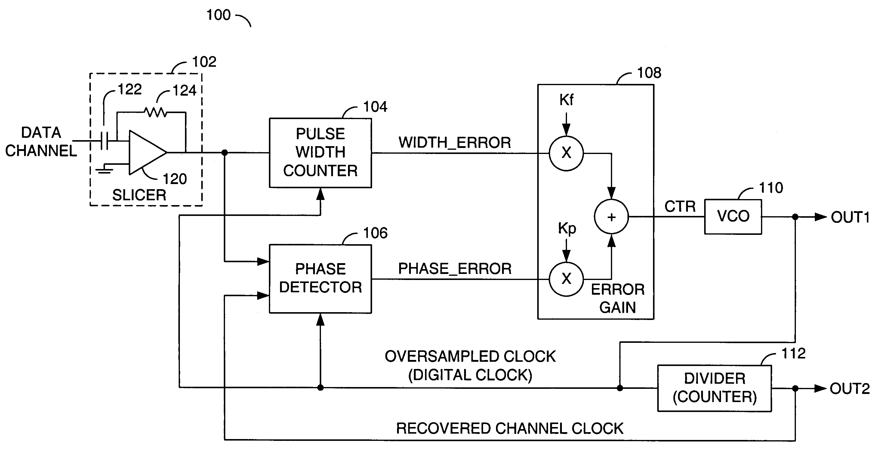
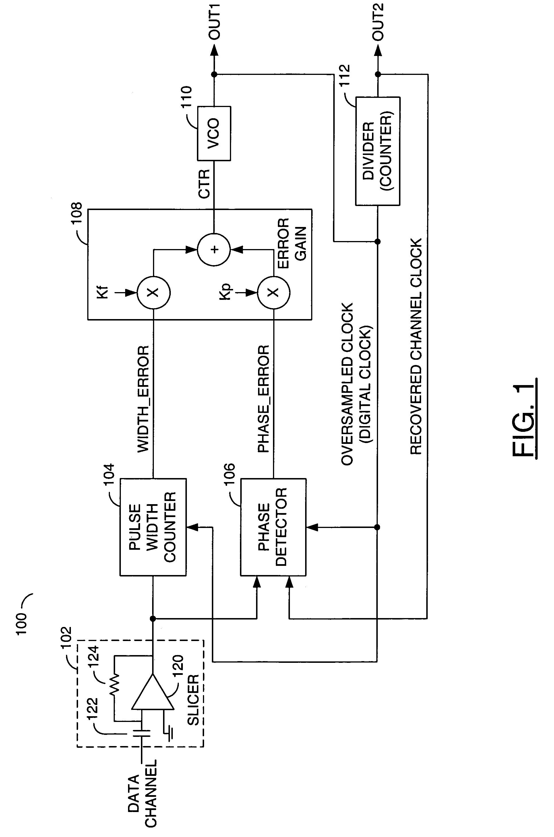
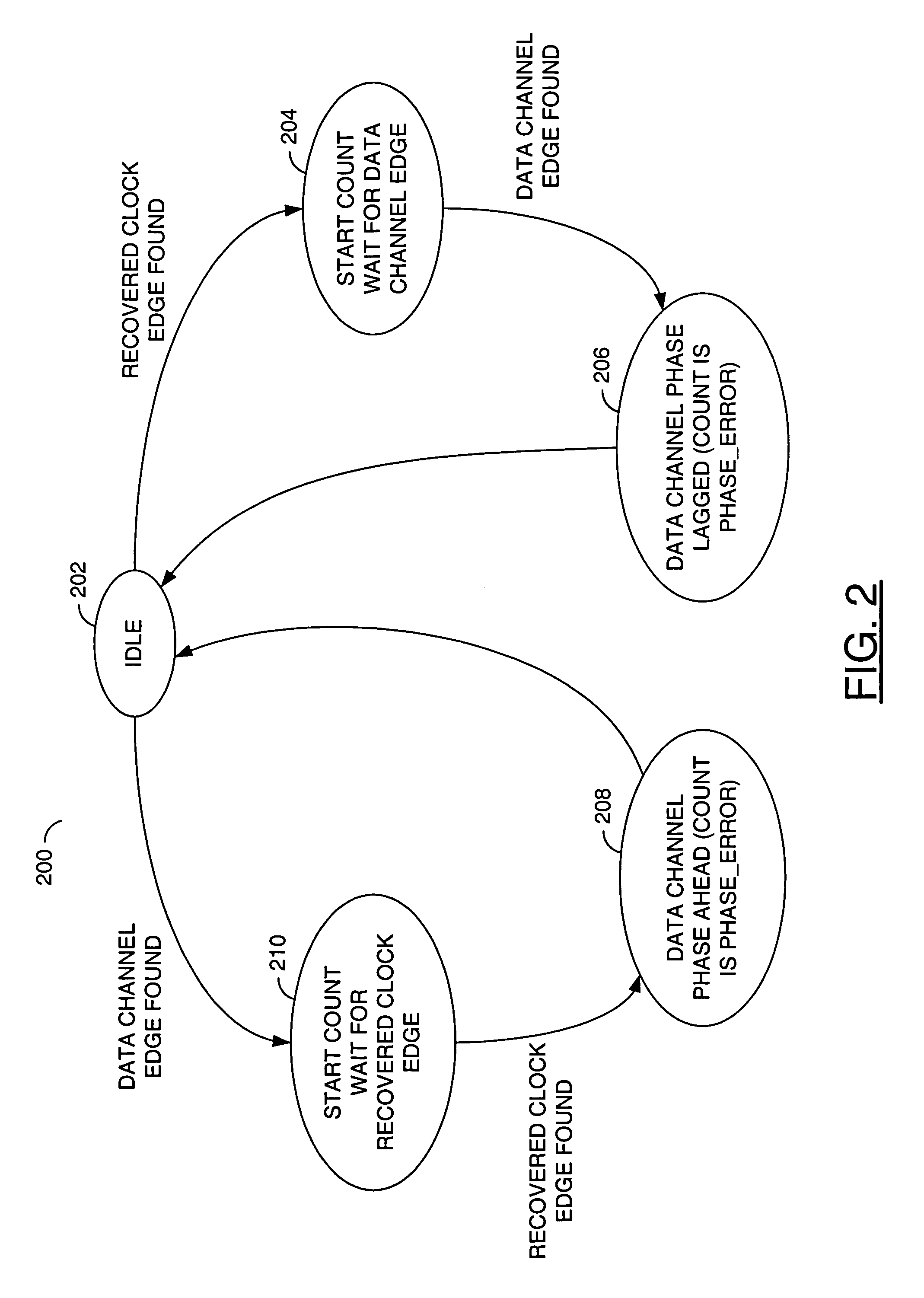
[0016]Referring to FIG. 1, a diagram of a circuit 100 is shown in accordance with a preferred embodiment of the present invention. The circuit 100 may be implemented as a clock recovery circuit. The circuit 100 generally comprises a block (or circuit) 102, a block (or circuit) 104, a block (or circuit) 106, a block (or circuit) 108, a block (or circuit) 110 and a block (or circuit) 112. The circuit 102 may be implemented as a slicer circuit. The circuit 104 may be implemented as a pulsewidth counter circuit. The circuit 106 may be implemented as a phase detector circuit. The circuit 108 may be implemented as an error gain circuit. The circuit 110 may be implemented as a voltage controlled oscillator circuit. The circuit 112 may be implemented as a divider circuit.

[0017]The slicer circuit 102 may receive an input signal (e.g., DATA_CHANNEL). The signal DATA_CHANNEL may be an input signal that includes data and an embedded clock signal. The slicer circuit 102 may couple the signal DAT...


PUM


Abstract

An apparatus comprising an oscillator circuit, a control circuit, a counter circuit and a detector circuit. The oscillator circuit may be configured to generate an output signal oscillating at a particular frequency in response to a control signal. The control circuit may be configured to generate the control signal in response to a first error signal and a second error signal. The counter circuit may be configured to generate the first error signal in response to the output signal and an input signal. The detector circuit may be configured to generate the second error signal in response to the output signal and the input signal.

Description

FIELD OF THE INVENTION[0001]The present invention relates to clock recovery generally and, more particularly, to a method and / or apparatus for implementing a low jitter and / or fast lock-in clock recovery circuit.BACKGROUND OF THE INVENTION[0002]Several conventional applications use clock recovery circuits in system on a chip (SOC) environments. Some examples include storage devices (i.e., optical disc and hard disc data retrieval) and serial data channels (i.e., USB, Firewire, serial ATAPI (SATA), etc.). In order to retrieve the data, the embedded data channel clock signal needs to be recovered and reconstructed from the incoming data. In conventional clock recovery systems, data bits are encoded in the data channel by transitions of the pulse edge using a format such as non return to zero (NRZ) or biphase encoding. Some serial data channel systems encode additional information, such as amplitude information, within the data channel. The additional information may be used either to ...

Claims


Application Information

Patent Timeline
Patent Type & Authority Patents(United States)
IPC IPC(8): H03D3/24
CPCH03L7/107H03L7/1075H03L7/113H04L7/033
Inventor LEUNG, HO-MINGPARVEEN, NASIMAKO, KA-SHU
Owner AVAGO TECH WIRELESS IP SINGAPORE PTE
Learn More