Triode structure field emission display device using carbon nanotubes and method of fabricating the same
a carbon nanotube and display device technology, applied in the manufacture of electrode systems, electric discharge tubes/lamps, discharge tubes luminescnet screens, etc., can solve the problem of reducing the amount of electrons emitted, difficult to achieve a high aspect ratio, and large amount of residues, etc. problem, to achieve the effect of suppressing the short circuit between electrodes
- Summary
- Abstract
- Description
- Claims
- Application Information
AI Technical Summary
Benefits of technology
Problems solved by technology
Method used
Image
Examples
first embodiment
[0050]FIGS. 5A through 5R are diagrams of a method of fabricating the field emission display device shown in FIG. 4 according to the present invention.
[0051]As shown in FIG. 5A, the cathode layer 112 of indium tin oxide (ITO) is deposited on the substrate 111. As described above, the cathode layer 112 is formed of a transparent conductive material for rear exposure.
[0052]Next, as shown in FIG. 5B, the insulation layer 115 is deposited on the cathode layer 112, and firing is performed at high temperature over 550° C. Unlike a conventional method of fabricating a field emission display device, in the first embodiment of the present invention, a mask cathode layer is removed; immediately the insulation layer 115 is deposited on the cathode layer 112; and a firing process is performed before forming a cathode pattern. Accordingly, an alignment error between the cathode pattern and a gate electrode pattern does not occur.
[0053]After the firing process, as shown in FIG. 5C, the gate elect...
second embodiment
[0063]FIGS. 7A through 7H are diagrams of a method of fabricating a field emission display device according to the present invention.
[0064]FIG. 7A shows a triode structure of a conventional field emission display device as shown in FIG. 2J. Reference numeral 211 denotes a substrate. Reference numeral 212 denotes an ITO electrode layer. Reference numeral 213 denotes a mask cathode layer. Reference numeral 215 denotes an insulation layer. Reference numeral 216 denotes a gate electrode. Reference numeral 218 denotes a well.
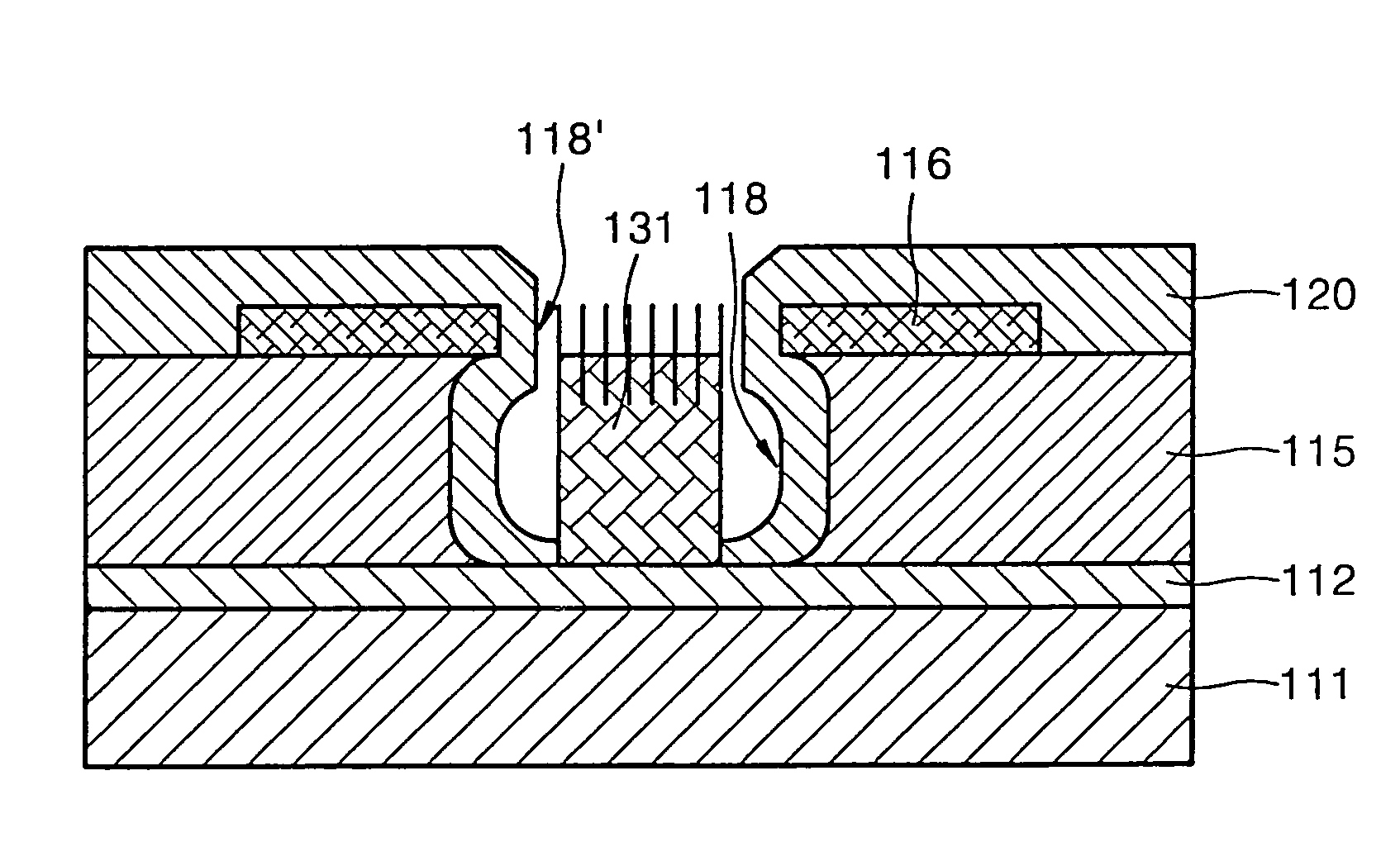
[0065]As shown in FIG. 7B, a material such as a dry film release (DFR) film which is a kind of photoresist and remains during developer treatment is deposited to cover the insulation layer 215 and the gate electrode 216, thereby forming a protective layer 217, and a mask 271 is disposed on the protective layer 217. Then, the protective layer 217 is patterned by a photoprocess including exposure and development, thereby forming a well 218′, as shown in FIG. 7C.
[0066]A...
PUM
| Property | Measurement | Unit |
|---|---|---|
| temperature | aaaaa | aaaaa |
| temperature | aaaaa | aaaaa |
| resistance | aaaaa | aaaaa |
Abstract
Description
Claims
Application Information
 - R&D
- Intellectual Property
- Life Sciences
- Materials
- Tech Scout
- Unparalleled Data Quality
- Higher Quality Content
- 60% Fewer Hallucinations
Browse by: Latest US Patents, China's latest patents, Technical Efficacy Thesaurus, Application Domain, Technology Topic, Popular Technical Reports.
© 2025 PatSnap. All rights reserved.Legal|Privacy policy|Modern Slavery Act Transparency Statement|Sitemap|About US| Contact US: help@patsnap.com


