Semiconductor optical device and manufacturing method thereof

a technology of semiconductors and optical devices, applied in semiconductor devices, semiconductor lasers, lasers, etc., can solve the problems of sharp deterioration of laser characteristics, suppress the diffusion of zn, and reduce the deterioration of crystallinity. , the effect of steep doping profil

Active Publication Date: 2009-04-07
LUMENTUM JAPAN INC
View PDF1 Cites 5 Cited by
  • Summary
  • Abstract
  • Description
  • Claims
  • Application Information

AI Technical Summary

Benefits of technology

[0008]The present invention is directed to reduce the deterioration of crystallinity in the vicinity of the active layer when doping C which is the p-type dopant, and to suppress the diffusion of Zn which is the p-type dopant to the undoped active layer, so as to realize a steep doping profile. With these effects, in the laser device structure, it is possible to reduce the device resistance while suppressing the increase of a threshold value current.
[0009]When a Zn-doped InGaAlAs layer having favorable crystallinity is formed between a C-doped InGaAlAs upper-side guiding layer and an undoped active layer, the influence of the C-doped InGaAlAs layer whose crystallinity is lowered can be reduced, in the vicinity of the active layer. Further, the diffusion of Zn from the Zn-doped InP cladding layer can be suppressed by the C-doped InGaAlAs layer. Further, as a result of studying the composition of the InGaAlAs and the deterioration of crystallinity during growth interruption, the C-doped layer is formed in the InGaAlAs composition with a small deterioration of crystallinity. FIG. 6 is a surface photograph during the growth interruption and FIG. 15 shows the summary of surface morphology. In the study, the InGaAlAs layer is grown on the InP substrate and the growth interruption is performed. While a surface of InAlAs having the large Al composition (Al: 0.48) forms a mirror surface, a surface of InGaAlAs having the small Al(aluminium) composition (Al: 0.25) forms pits therein. Hence, the surface of InGaAs is milky. The surface morphology has a tendency to become a mirror surface along with the increase of the Al composition. By performing the growth interruption in the InAlAs composition or in the InGaAlAs composition close to the InAlAs composition, the deterioration of the crystallinity can be reduced. Thus, with the Zn-doped InGaAlAs layer formed on the active layer, and the C-doped InGaAlAs layer with lowered crystallinity separated from the active layer, it is possible to reduce the influence of loss of the crystallinity. Further, it is possible to reduce the occurrence of defects due to the growth interruption by providing the growth interruption by the C-doped layer to the inside of the InGaAlAs layer or the InAlAs layer which contains the large Al composition.
[0010]According to the present invention, it is possible to achieve both of the reduction of the deterioration of crystallinity in the vicinity of the active layer due to C doping and the reduction of Zn diffusion from the cladding layer to the active layer. This improves a manufacturing yield rate, reduces a threshold current value, and increases an optical output.

Problems solved by technology

However, when the concentration of Zn becomes excessively high, Zn diffuses into an undoped active layer and hence, the laser characteristic is sharply deteriorated. FIG. 13 shows a result of an experiment on Zn characteristic by actually preparing laser devices.

Method used


Image

  • Semiconductor optical device and manufacturing method thereof
  • Semiconductor optical device and manufacturing method thereof
  • Semiconductor optical device and manufacturing method thereof

Examples


embodiment 1

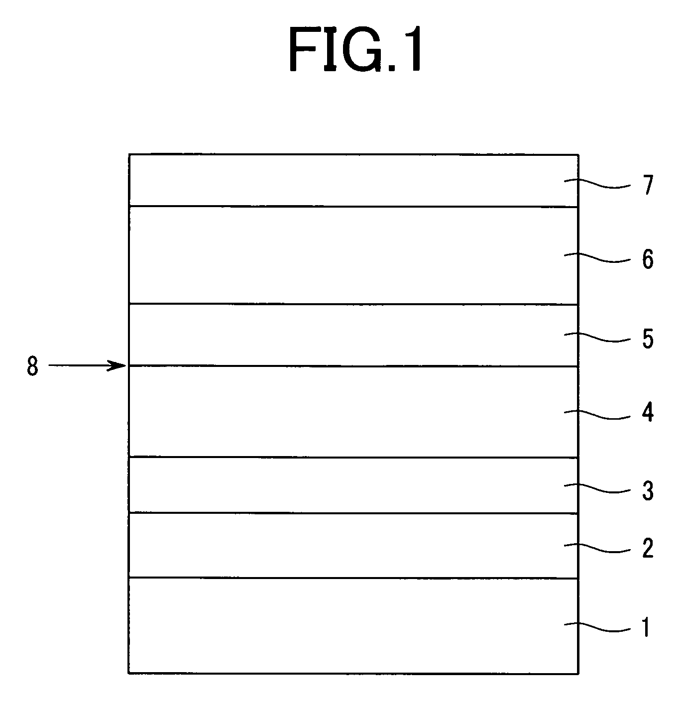
[0027]FIG. 7 shows the cross-sectional structure of the present invention. The following layers are successively grown on an n-InP. substrate 1 by metalorganic vapor phase epitaxy: an n-InP cladding layer 2, an n-InGaAlAs lower-side guiding layer 3, an undoped InGaAlAs multiple quantum well active layer 4, a Zn-doped InGaAlAs upper-side guiding layer 9, a Zn-doped InGaAlAs composition gradient layer (an InGaAlAs layer to an InAlAs layer) 10, a C-doped InAlAs cladding layer (C: 1 to 5×1018 cm−3) 11, a Zn-doped InP cladding layer (Zn: 1×1018 cm−3) 6, and a Zn-doped InGaAs contact layer 7 (Zn: 2×1018 cm−3). The layers up to the Zn-doped InGaAlAs upper-side guiding layer 9 are continuously grown at a growth temperature of 690° C. Then, since it is necessary to lower the growth temperature to 570° C. prior to the growth of the C-doped InAlAs cladding layer 11, the growth interruption 8 is provided. After the growth temperature is stabilized, the C-doped InAlAs cladding layer 11 is grown....

embodiment 2

[0029]FIG. 8 shows an example in which the present invention is applied to a case where the semiconductor optical device includes an upper-side grating layer. When an InGaAsP layer is doped with C, C becomes a p-type dopant in the vicinity of an InGaAs layer and becomes an n-type layer with a low doping concentration (approximately 1×1016 cm−3) in the vicinity of an InP layer. Further, when the InGaAlAs layer is formed of a grating layer, it is necessary to cope with oxidation of a re-growth interface since the grating layer contains Al. Accordingly, with respect to the device structure, an n-InP cladding layer 2, an n-InGaAlAs lower-side guiding layer 3, an undoped InGaAlAs multiple quantum well active layer 4 and a Zn-doped InGaAlAs upper-side guiding layer 9 are grown on an n-InP substrate 1 in the same manner as the above-mentioned embodiment 1. Thereafter, growth interruption by lowering the temperature, growth of a C-doped InAlAs layer 11, growth interruption by increasing the...

embodiment 3

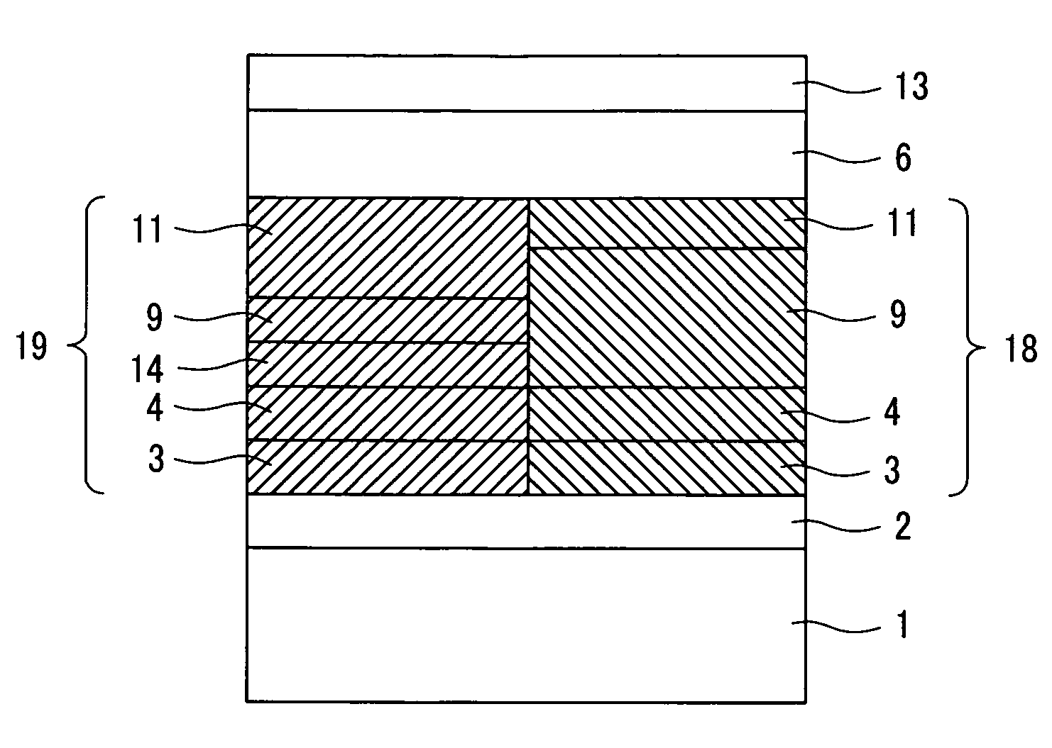
[0030]FIG. 9 shows a case where the present invention is applied to an integrated light source which is formed by a laser and an electro absorption modulator. In the same manner as the above-mentioned embodiment 1, an n-InP cladding layer 2, an n-InGaAlAs lower-side guiding layer 3, an undoped InGaAlAs multiple quantum well active layer 4, a Zn-doped InGaAlAs upper-side guiding layer 9, a C-doped InAlAs cladding layer 11, and a portion of a Zn-doped InP cladding layer are grown on an n-InP substrate 1, forming a laser part 18. Thereafter, using an oxide as a mask, the structure ranging from the surface layer to the substrate is etched by dry etching or wet etching. An n-InGaAlAs lower-side guiding layer 3, an undoped InGaAlAs multiple quantum well active layer 4, an undoped InGaAlAs layer upper-side guiding layer 14, a Zn-doped InGaAlAs upper-side guiding layer 9, a C-doped InAlAs cladding layer 11, and a portion of an InP cladding layer are formed on the removed portion, forming an...


PUM


Abstract

The object of the invention is to reduce the deterioration of crystallinity in the vicinity of an active layer when C, which is a p-type dopant, is doped and to suppress the diffusion of Zn, which is a p-type dopant, into an undoped active layer, thus to realize a sharp doping profile. When a Zn-doped InGaAlAs layer having favorable crystallinity is provided between a C-doped InGaAlAs upper-side guiding layer and an undoped active layer, the influence of the C-doped InGaAlAs layer whose crystallinity is lowered can be reduced in the vicinity of the active layer. Further, the Zn diffusion from a Zn-doped InP cladding layer can be suppressed by the C-doped InGaAlAs layer.

Description

PRIORITY OF CLAIMS[0001]The present application claims priority from Japanese application JP2006-168827, filed on Jun. 19, 2006, the content of which is hereby incorporated by reference into this application.BACKGROUND OF THE INVENTION[0002]1. Field of the invention[0003]The present invention relates to semiconductor optical devices and a manufacturing method thereof, and more particularly to a technique which is effectively applicable to the structure of a p-type semiconductor layer of a semiconductor optical device including a semiconductor laser, and a method for forming the p-type semiconductor layer.[0004]2. Description of the Related Arts[0005]As a method of crystal growth on an InP substrate for a semiconductor laser, a metalorganic vapor phase epitaxy has been mainly used. Zn is used as a p-type dopant, which is produced from DEZn or DMZn, and Si or Se is used as an n-type dopant, which are produced from Si2H6 or H2Se. Although Si and Se used as the n-type dopants hardly dif...

Claims


Application Information

Patent Timeline
Patent Type & Authority Patents(United States)
IPC IPC(8): H01L21/28
CPCB82Y20/00H01S5/305H01L33/305H01S5/0265H01S5/2226H01S5/2275H01S5/3054H01S5/3211H01S5/3215H01S5/34313
Inventor SHIOTA, TAKASHITSUCHIYA, TOMONOBU
Owner LUMENTUM JAPAN INC
Why Eureka
Try Eureka