Method and system for detection of wafer centering in a track lithography tool
a lithography tool and track technology, applied in the field of substrate processing equipment, can solve problems such as unwanted contact between optical elements and processing fluids, and achieve the effect of small form factor
- Summary
- Abstract
- Description
- Claims
- Application Information
AI Technical Summary
Benefits of technology
Problems solved by technology
Method used
Image
Examples
Embodiment Construction
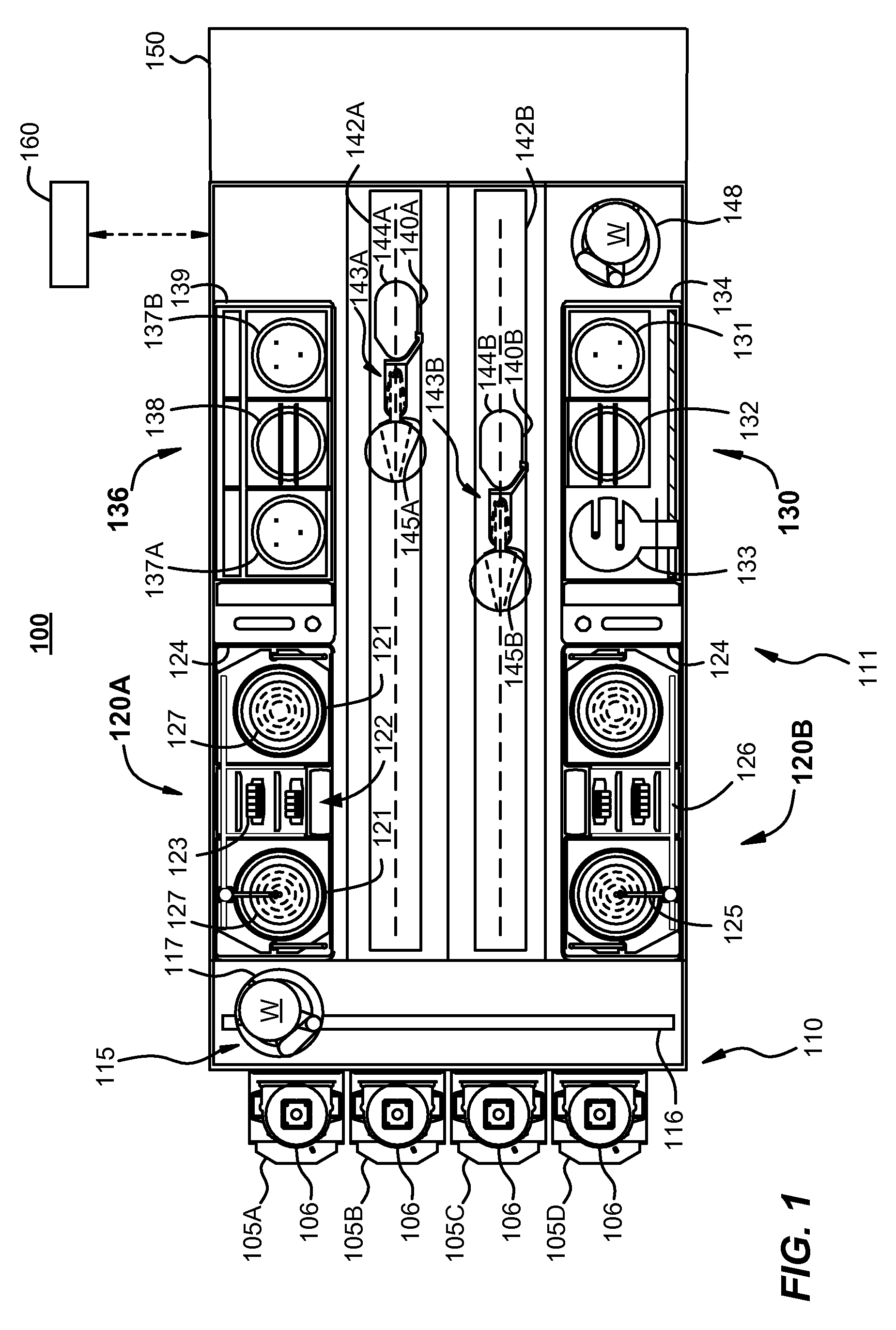
[0022]FIG. 1 is a plan view of an embodiment of a track lithography tool in which the embodiments of the present invention may be used. As illustrated in FIG. 1, the track lithography tool contains a front end module 110 (sometimes referred to as a factory interface) and a process module 111. In other embodiments, the track lithography tool includes a rear module (not shown), which is sometimes referred to as a scanner interface. Front end module 110 generally contains one or more pod assemblies or FOUPS (e.g., items 105A-D) and a front end robot assembly 115 including a horizontal motion assembly 116 and a front end robot 117. The front end module 110 may also include front end processing racks (not shown). The one or more pod assemblies 105A-D are generally adapted to accept one or more cassettes 106 that may contain one or more substrates or wafers that are to be processed in the track lithography tool. The front end module 110 may also contain one or more pass-through positions ...
PUM
 Abstract
Description
Claims
Application Information
 - R&D
- Intellectual Property
- Life Sciences
- Materials
- Tech Scout
- Unparalleled Data Quality
- Higher Quality Content
- 60% Fewer Hallucinations
Browse by: Latest US Patents, China's latest patents, Technical Efficacy Thesaurus, Application Domain, Technology Topic, Popular Technical Reports.
© 2025 PatSnap. All rights reserved.Legal|Privacy policy|Modern Slavery Act Transparency Statement|Sitemap|About US| Contact US: help@patsnap.com


