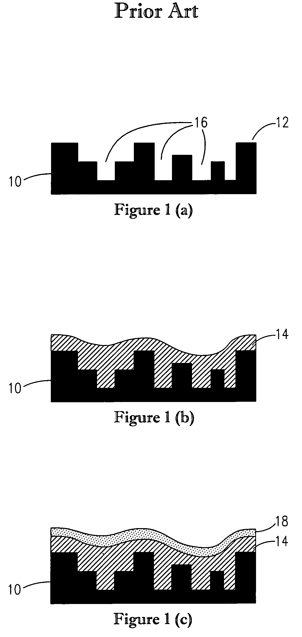
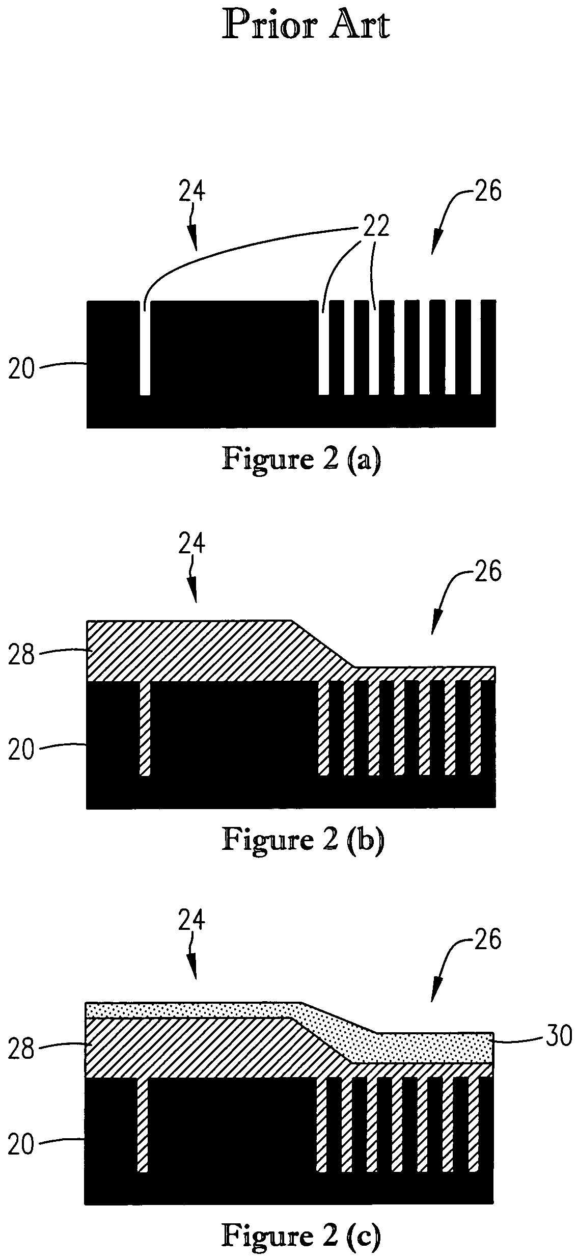
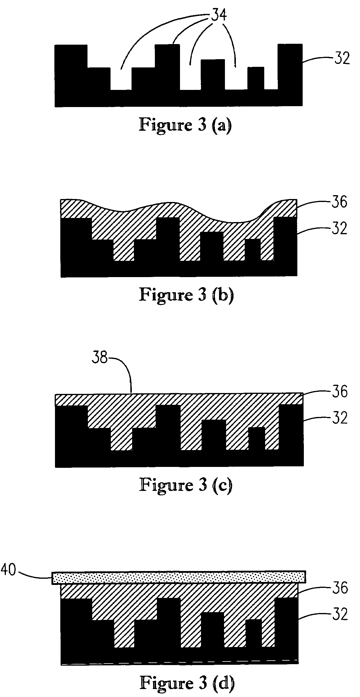
Planarization method for multi-layer lithography processing
a multi-layer lithography and planarization technology, applied in the direction of photosensitive materials, instruments, electric/magnetic/electromagnetic heating, etc., can solve the problems of fine feature sizes that cannot be patterned on the substrate surface, the topography of the substrate is so severe, and the lithography process is beyond the limits of what is possible, etc., to prevent problems or inhibit problems
- Summary
- Abstract
- Description
- Claims
- Application Information
AI Technical Summary
Benefits of technology
Problems solved by technology
Method used
Image

Examples
example 1
Photo-Curable Planarization Material on a Via Wafer
[0040]A photo-curable material was prepared by mixing of 20 g of epoxy (D.E.R. 354LV, The Dow Chemical Co.), 80 g of PGME (Aldrich), and 1.2 g of Sarcat KI-85 (a photoacid generator available from Sartomer) in a yellow-lighted laboratory. The material was filtered with a 0.2-μm filter and stored in a clean brown bottle.
[0041]A via-containing silicon wafer was used as the substrate. The silicon wafer was first coated with a silicon dioxide film having a thickness of about 1 μm. A pattern having areas of various feature densities and having vias that were 0.2 to 1 μm in diameter was formed in the silicon dioxide film. The via depth was about 1 μm.
[0042]A film of photo-curable planarization material having a thickness of about 0.4 μm was spin-coated onto the via wafer having various pattern feature density areas. The wafer was transferred to a press tool chamber and placed on a substrate stage. The top surface of the planarization mate...
example 2
Photo-Curable Planarization Material on a Trench Wafer
[0045]A photo-curable material was prepared by thoroughly mixing 20 g of epoxy (D.E.R. 354LV, The Dow Chemical Co.), 80 g of PGME (Aldrich), and 1.2 g of Sarcat KI-85 (Sartomer) in a yellow-lighted laboratory. The material was then filtered with a 0.2-μm filter and stored in a clean brown bottle.
[0046]A silicon wafer having trench structures that were about 1 μm deep was used as the substrate. The feature density of this wafer ranged from 4% to 96%.
[0047]A film of photo-curable planarization material less than 0.5 μm thick was spin-coated onto the silicon trench wafer which included different feature density areas. The wafer was transferred to a press tool chamber and placed on a substrate stage. The coated substrate surface was oriented to face an optically transparent optical flat object surface. The chamber lid was sealed, and the chamber was evacuated to less than 20 Torr. The chamber pressure was maintained at less than 20 T...
example 3
Thermo-Curable Planarization Material on a Via Wafer
[0050]A thermo-curable material was prepared by mixing 20 g of epoxy (D.E.R. 354LV, The Dow Chemical Co.), 80 g of PGME (Aldrich), and 1.0 g of NACURE Super XC-A230 Catalyst (a thermo-acid generator, available from King Industries) were prepared and mixed thoroughly. The material was filtered with a 0.2-μm filter and stored in a clean brown bottle.
[0051]A via-containing silicon wafer was used as the substrate. The silicon wafer was first coated with a silicon dioxide film having a thickness of about 1 μm. A pattern containing vias of 0.2 to 1 μm in diameter and having various feature density areas was patterned into the silicon dioxide film. The depth of the vias was about 1 μm.
[0052]A film of thermo-curable planarization material having a thickness of about 0.2 μm was spin-coated onto the silicon via wafer having different feature density areas. The wafer was transferred to a press tool chamber and placed on a substrate stage. The...
PUM
| Property | Measurement | Unit |
|---|---|---|
| Temperature | aaaaa | aaaaa |
| Length | aaaaa | aaaaa |
| Time | aaaaa | aaaaa |
Abstract
Description
Claims
Application Information
 - R&D
- Intellectual Property
- Life Sciences
- Materials
- Tech Scout
- Unparalleled Data Quality
- Higher Quality Content
- 60% Fewer Hallucinations
Browse by: Latest US Patents, China's latest patents, Technical Efficacy Thesaurus, Application Domain, Technology Topic, Popular Technical Reports.
© 2025 PatSnap. All rights reserved.Legal|Privacy policy|Modern Slavery Act Transparency Statement|Sitemap|About US| Contact US: help@patsnap.com