Apparatus and method for reducing flicker noise of CMOS amplifier

a technology of cmos amplifier and cmos, which is applied in the direction of amplifiers with semiconductor devices/discharge tubes, amplifiers with different amplifiers, and amplifier modifications to reduce noise influence, etc., can solve the problems of l/f noise, and user inconvenience, so as to reduce the low frequency flicker noise

Active Publication Date: 2008-11-18
SAMSUNG ELECTRONICS CO LTD
View PDF12 Cites 6 Cited by
  • Summary
  • Abstract
  • Description
  • Claims
  • Application Information

AI Technical Summary

Benefits of technology

[0009]The present invention provides a CMOS amplifier which can be applied to the processing of a continuous signal and also can reduce a low frequency flicker noise such as a glitch.
[0010]The present invention also provides a method of processing a continuous signal to reduce a low frequency flicker noise.

Problems solved by technology

While the communication system described above requires a high signal-to-noise (SNR) ratio, devices which constitute the CMOS amplifier 100 are being down-scaled and a low frequency flicker noise caused by this physical property, i.e. l / f noise, is annoying to users.
However, in this case, since parasitic components increase, an operating frequency may be limited.
However, it is difficult to process a continuous input signal VIN due to the clock signals Ø1 and Ø2.

Method used


Image

  • Apparatus and method for reducing flicker noise of CMOS amplifier
  • Apparatus and method for reducing flicker noise of CMOS amplifier
  • Apparatus and method for reducing flicker noise of CMOS amplifier

Examples


Embodiment Construction

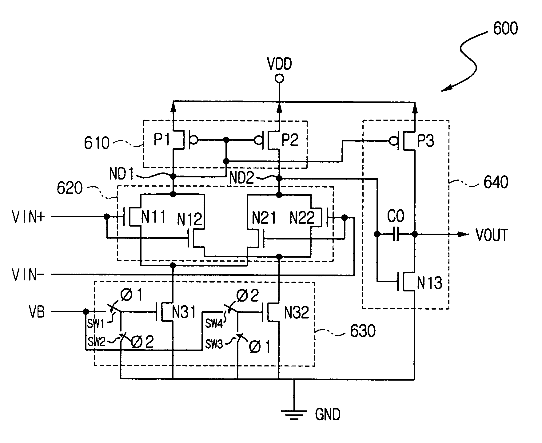
[0030]Reference will now be made in detail to exemplary embodiments of the present invention, examples of which are illustrated in the accompanying drawings, wherein like reference numerals refer to the like elements throughout. The exemplary embodiments are described below in order to explain the present invention by referring to the figures.

[0031]FIG. 4 illustrates a circuit 400 for measuring a flicker noise of a MOSFET 410. After driving a gate G of the MOSFET 410 via a clock pulse 420 and supplying a certain current iD via a certain circuit 430, a current flowing between a drain D and a source S is measured. In this instance, as the gate G of the MOSFET 410 is driven by the clock pulse 420, a current inoise by a l / f low frequency flicker noise reduces the current flowing between the drain D and the source S.

[0032]As an example, as depicted in the graph shown in FIG. 5, a power of a l / f noise which shows a greater flicker noise in a lower frequency is decreased when adding the cl...


PUM


Abstract

An apparatus and method of reducing a flicker noise of a CMOS amplifier is provided. In the CMOS amplifier, a load circuit is connected to a signal input circuit which includes two pairs of MOSFETs which simultaneously receive differential signals. In this instance, a first MOSFET included in a switch-bias circuit is connected to one pair of MOSFETs which receive the differential signals and functions as a current source in the case of activation of a clock signal Ø1. A second MOSFET included in the switch-bias circuit is connected to another pair of MOSFETs which receive the differential signals and functions as a current source in the case of activation of a clock signal Ø2.

Description

CROSS-REFERENCE TO RELATED APPLICATION[0001]This application claims priority from Korean Patent Application No. 10-2005-01130977, filed on Dec. 27, 2005, in the Korean Intellectual Property Office, the disclosure of which is incorporated herein by reference.BACKGROUND OF THE INVENTION[0002]1. Field of the Invention[0003]Methods and apparatuses consistent with the present invention relate to a complementary metal-oxide semiconductor (CMOS) amplifier, and more particularly, to an apparatus and method which can reduce a low frequency flicker noise in the CMOS amplifier.[0004]2. Description of Related Art[0005]With increasing developments in the field of a semiconductor technology, the size of devices which constitute a semiconductor circuit, such as a CMOS amplifier, is being reduced. As shown in FIG. 1, a CMOS amplifier 100 in the form of a differential amplifier which amplifies input differential signals V+ and V−, and outputs an amplified signal VOUT, is widely utilized in circuits ...

Claims


Application Information

Patent Timeline
Patent Type & Authority Patents(United States)
IPC IPC(8): H03F3/45
CPCH03F1/26H03F3/45183H03F3/45
Inventor KOH, JEONG WOOKCHAE, HYUN SOOKIM, HOON TAE
Owner SAMSUNG ELECTRONICS CO LTD
Why Eureka
Try Eureka