
Forming composite metal oxide layer with hafnium oxide and titanium oxide

a technology of titanium oxide and composite metal oxide, which is applied in the direction of coatings, chemical vapor deposition coatings, semiconductor devices, etc., can solve the problems of complex structure manufacturing of the lower electrode of the capacitor having the cylindrical shape or the fin shape, and the capacitance may not be obtained for stably operating the cell in the semiconductor device such as the dynamic random access memory (dram) device, so as to improve the leakage current characteristics and high dielectric constant

Active Publication Date: 2008-09-23
SAMSUNG ELECTRONICS CO LTD
View PDF7 Cites 5 Cited by
  • Summary
  • Abstract
  • Description
  • Claims
  • Application Information

AI Technical Summary

Benefits of technology

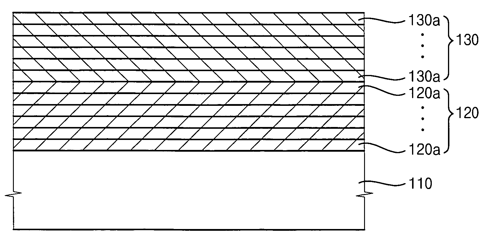
The present invention provides a method of forming a metal oxide alloy layer with improved leakage current characteristics and a high dielectric constant. This layer can be used in the manufacturing of gate structures and capacitors with improved performance. The method involves forming layers of metal oxides on a substrate, allowing them to move into each other to create a single-layered structure. This results in a more effective barrier to leakage current and a higher dielectric constant, which can improve the performance of the final product.

Problems solved by technology

As a result of the reduced-size cell region, a sufficient capacitance for stably operating a cell in a semiconductor device such as a dynamic random access memory (DRAM) device may not be obtained.
However, the lower electrode of the capacitor having the cylindrical shape or the fin shape is a complicated structure to manufacture.

Method used


Image

  • Forming composite metal oxide layer with hafnium oxide and titanium oxide
  • Forming composite metal oxide layer with hafnium oxide and titanium oxide
  • Forming composite metal oxide layer with hafnium oxide and titanium oxide

Examples


Embodiment Construction

[0023]Exemplary embodiments of the present invention will be described below in more detail with reference to the accompanying drawings. The present invention may be embodied in many different forms and should not be construed as limited to the embodiments set forth herein.

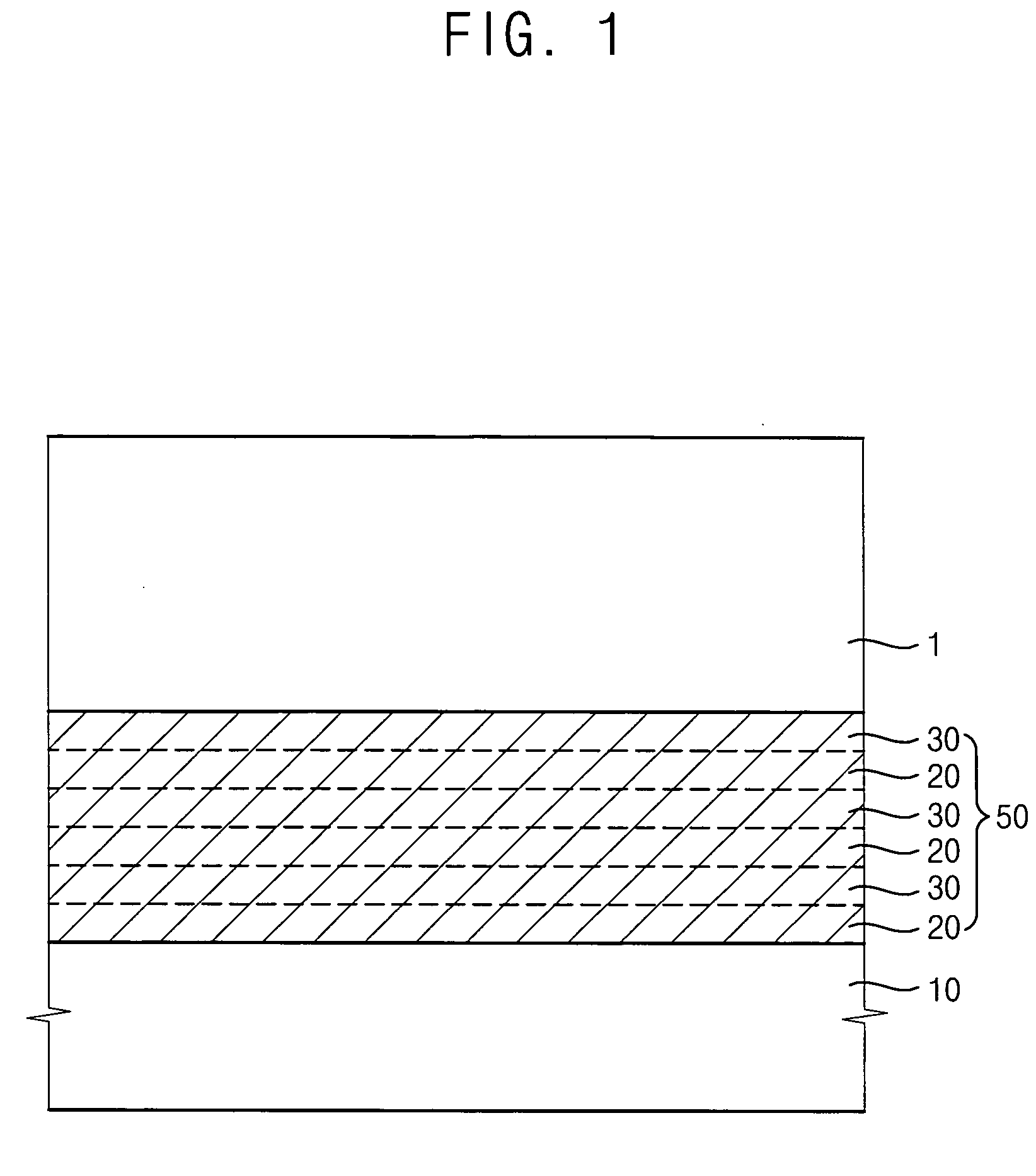
[0024]FIG. 1 is a cross-sectional view illustrating a metal oxide alloy layer in accordance with an embodiment of the present invention.

[0025]Referring to FIG. 1, a metal oxide alloy layer 50 includes a single-layered structure in which metal oxides from different metal oxide layers are mixed.

[0026]The metal oxide alloy layer 50 includes first layers 20 having a first metal oxide alternately stacked with second layers 30 having a second metal oxide that are alternately stacked. The first layer 20 has a first thickness for allowing the first metal oxide to escape from the first layer 20. The second layer 30 has a second thickness for allowing the second metal oxide to escape from the second layer 30. Thus, the firs...


PUM

PropertyMeasurementUnit
temperatureaaaaaaaaaa
dielectric constantaaaaaaaaaa

Abstract

A metal oxide alloy layer comprises a first layer including a first metal oxide and having a first thickness, and a second layer formed on the first layer, the second layer including a second metal oxide and having a second thickness, wherein a value of the first thickness is such that the first metal oxide is allowed to move into the second layer and a value of the second thickness is such that the second metal oxide is allowed to move into the first layer to form a single-layered structure in which the first and second metal oxides are mixed.

Description

CROSS-REFERENCE TO RELATED APPLICATION[0001]This application claims priority to Korean Patent Application No. 2005-2168, filed on Jan. 10, 2005, the contents of which are herein incorporated by reference in their entirety.BACKGROUND OF THE INVENTION[0002]1. Technical Field[0003]The present disclosure relates to a metal oxide alloy layer, and more particularly, to a metal oxide alloy layer having a structure in which at least two kinds of metal oxides are mixed and methods of forming the same.[0004]2. Discussion of the Related Art[0005]As semiconductor devices become highly integrated, a size of a cell region is reduced. As a result of the reduced-size cell region, a sufficient capacitance for stably operating a cell in a semiconductor device such as a dynamic random access memory (DRAM) device may not be obtained. As shown in the following Equation 1, the capacitance C is proportional to a dielectric constant ε and areas A of electrodes, and is inversely proportional to a distance d...

Claims


Application Information

Patent Timeline
Patent Type & Authority Patents(United States)
IPC IPC(8): H01L29/78H01L21/31H10B12/00
CPCC23C16/403C23C16/405C23C16/45531H01L21/28194H01L29/517H01L21/3142H01L21/31604H01L21/31616H01L21/31645H01L21/02178H01L21/02181H01L21/022H01L21/0228H01L21/02186H01L21/02189H01L21/02194H01L21/18H10B99/00
Inventor LEE, JUNG-HOCHOI, JUNG-SIKCHO, JUN-HYUNEOM, TAE-MINLEE, JI-HYUN
Owner SAMSUNG ELECTRONICS CO LTD
Learn More