
Substrate processing method

a substrate processing and substrate technology, applied in the direction of photosensitive material processing, lighting and heating apparatus, cleaning using liquids, etc., can solve the problems of affecting the production efficiency of substrates, uneven thickness, and poor film quality, so as to facilitate the removal of resists, suppress the growth of chemical oxide films, and suppress metal contamination of wafers

Inactive Publication Date: 2008-08-12
TOKYO ELECTRON LTD
View PDF19 Cites 3 Cited by
  • Summary
  • Abstract
  • Description
  • Claims
  • Application Information

AI Technical Summary

Benefits of technology

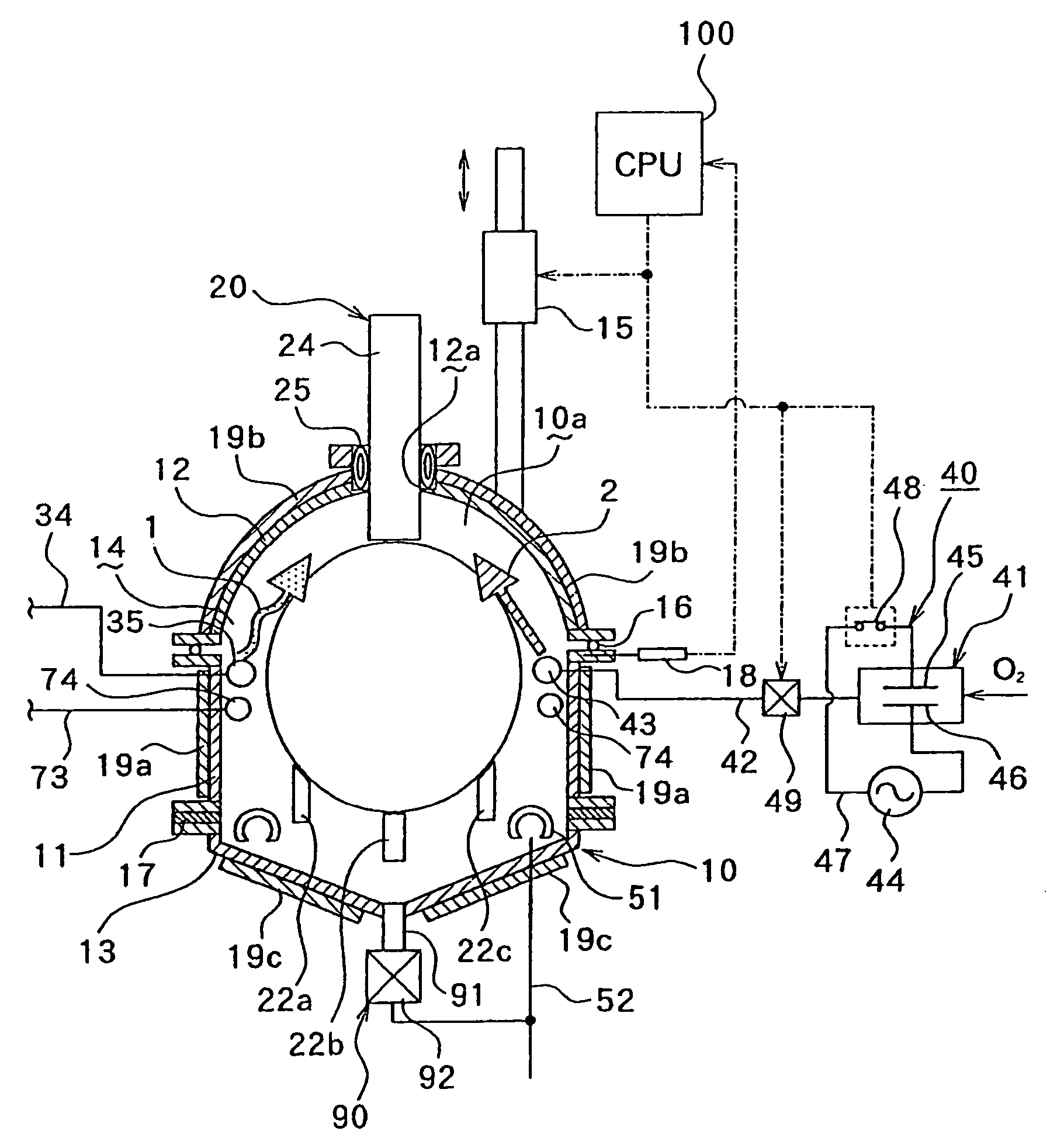
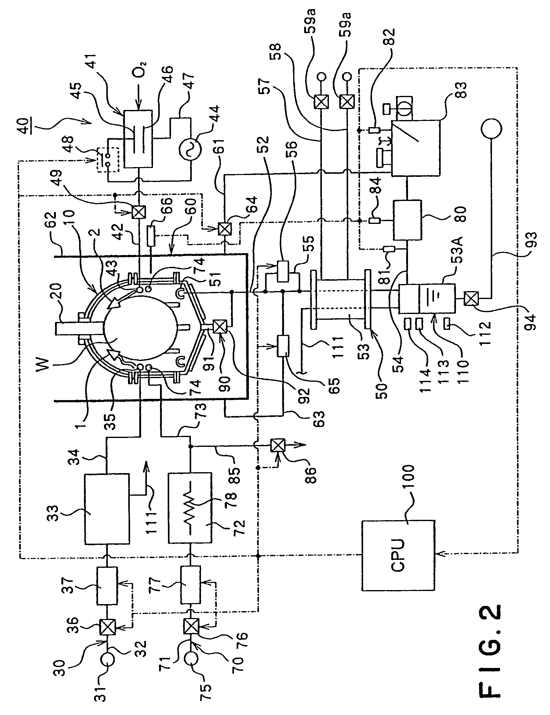
[0014]The present invention was made in view of the above-described problems, and an object of the present invention is to provide a substrate processing method and a substrate processing apparatus which can facilitate the removal of resists while suppressing the metal contamination of wafers or others and the generation of particles, and suppressing the growth of chemical oxide films on the surfaces of the wafers or others.
[0018]In the substrate processing method and the substrate processing apparatus according to the present invention, before a processing gas is fed to the processing vessel to process the substrate-to-be-processed, the processing gas is fed into the processing vessel to pressurize the atmosphere surrounding the substrates, whereby the atmosphere in the processing vessel is replaced by an atmosphere of the processing gas while the interior of the processing vessel is pre-pressurized. Accordingly, the risk that the substrate-to-be-processed may contact gases, etc. other than the processing gas is avoided, and metal contamination and generation of particles can be accordingly prevented. Rates of the reaction between solvent vapor and the processing gas fed subsequently into the processing vessel are increased to thereby improve efficiency of the processing.

Problems solved by technology

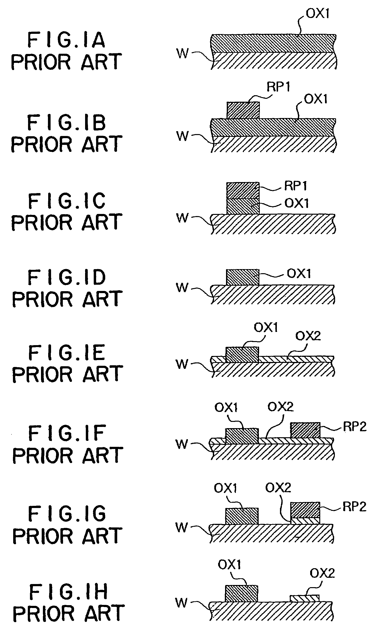
However, when sulfonated water is used as the chemical liquid in the first resist removing step (see FIG. 1D), sulfuric acid ions remain on the surface of the wafer W after the resist has been removed, and there is a risk that the residual sulfuric acid ions may become a cause for particles and cause contamination.
Furthermore, the residual sulfuric acid ions also causes an uneven thickness and poor film quality of the thin oxide film formed in the following second oxide film forming step (see FIG. 1E).
It is often that meanwhile ozone in the solution is decomposed, and the solution has the ozone concentration decreased, and a sufficient amount of ozone cannot be supplied to the resist surface.
High reaction rates cannot be provided.
When nitrogen contacts the wafers or others, the nitrogen reacts with the ozone gas to corrode and etch metals of aluminum (Al) and tungsten (W) of the wiring portions, causing particles.
This problem of the metal contamination and particle generation is the case also with the wafers or others which have not been subjected to the wiring step.
The processing with ozone gas containing nitrogen excessively oxidizes the wafers or others with NOx- or HNOx-based atmospheres (chemicals), and chemical oxide films grow on the surfaces of the wafers or others, possibly causing thickness unevenness and poor film quality of the thin oxide film.

Method used


Image

  • Substrate processing method
  • Substrate processing method
  • Substrate processing method

Examples


example 1

[0084]Experiments were made under the following conditions on etching rates of metals in the case where ozone gas contains nitrogen (N2) and in the case where ozone gas contains no nitrogen (N2).

[0085]Experiment Conditions:

[0086]A) Specimen metals: aluminum (Al), copper (Cu) and tungsten (W)

[0087]B) Processing conditions:

[0088]1) For the case where ozone gas contains nitrogen (N2):[0089]Pressure: 70.0[kPa][0090]Wafer temperature: 80[°C.][0091]Steam temperature: 115[°C.][0092]Processing period of time: 5 [min]

[0093]2) For the case where ozone gas contains no nitrogen (N2):[0094]Pressure: 70.0[kPa][0095]Wafer temperature: 80[°C.][0096]Steam temperature: 115[°C.][0097]Processing period of time: 5 [min]

[0098]The experiments were conducted under the above-described conditions, and the results of the experiments are as shown in FIG. 10.

[0099]The aluminum (Al) specimen had an etching rate of 86.38 [angstrom / min] in the case where ozone gas contained nitrogen (N2), and in the case where ozo...

example 2

[0101]Experiments were made under the following conditions on growth rates of chemical oxide films in cases of resist removal processing using ozone gas having different nitrogen addition amounts (contents).[0102]Ozone gas: 10 l / min (N2 added; No N2 added)[0103]Steam: 120° C.[0104]Wafer temperature: 90° C.[0105]Pressure: 0.05 MPa (Zero-adjusted atmospheric pressure (0.1 MPa))[0106]Ozone gas / steam feed period of time: 5 minutes[0107]N2 feed rate: 0.08 l / min

[0108]The experiments were made under the above-described conditions, and the results shown in TABLE 1 were obtained.

[0109]

TABLE 1Oxide filmOxide filmOxide filmthicknessthicknessgrowthbefore processedafter processedamountProcessed with3.3516.9013.55ozone gas with[angstrom][angstrom][angstrom]N2 addedprocessed with3.7011.237.54ozone gas with-[angstrom][angstrom][angstrom]out N2 added

[0110]According to the results of the above-described experiments, in the case where the resist removing processing was performed with ozone gas (O3 con...


PUM

PropertyMeasurementUnit
temperatureaaaaaaaaaa

Abstract

Resists can be removed while metal contamination of wafers, etc. and generation of particles, and growth of oxide films are suppressed. A substrate processing method comprises feeding a processing gas, such as ozone gas, into a processing vessel to pressurize an atmosphere surrounding a substrate. A solvent gas, such as steam, is fed into the processing vessel while the processing gas is fed into the processing vessel, whereby a resist of the substrate can be removed with the solvent gas and the processing gas while metal corrosion, etc. can be prevented.

Description

CROSS-REFERENCE TO RELATED APPLICATIONS[0001]This application is a division of application Ser. No. 09 / 971,136 filed on Oct. 3, 2001, now U.S. Pat. No. 6,817,368 and is related to subject matter disclosed in Japanese Patent Application No. 2000-304375 filed on Oct. 4, 2000 in Japan and Japanese Patent Application No. 2001-41482 filed on Feb. 19, 2001 to which this application claims priority under Paris Convention, and which all three are specifically incorporated herein by reference.BACKGROUND OF THE INVENTION[0002]1. Field of the Invention[0003]The present invention relates to a substrate processing method and a substrate processing apparatus, more specifically, a substrate processing method and a substrate processing apparatus for processing substrate-to-be-processed, such as semiconductor wafers, LCD glass substrates or others, held in an atmosphere sealed processing vessel with a processing gas, such as ozone, etc., fed into the processing vessel.[0004]2. Related Background Art...

Claims


Application Information

Patent Timeline
Patent Type & Authority Patents(United States)
IPC IPC(8): B08B3/00B08B5/00G03F7/42H01L21/00H01L21/027H01L21/302H01L21/304H01L21/3065H01L21/311
CPCH01L21/31138H01L21/6708Y10S134/902H01L21/304
Inventor TOSHIMA, TAKAYUKISHINDO, NAOKIIINO, TADASHI
Owner TOKYO ELECTRON LTD
Learn More