
Light emitting element and manufacturing method thereof, and light emitting device using the light emitting element

a technology manufacturing methods, applied in the field of light emitting elements, can solve the problems of reducing the external extraction efficiency of emitted light, unable to obtain favorable characteristics, and unable to achieve luminous efficiency in red light emission, etc., and achieves the effect of suppressing the short circuit between electrodes

Inactive Publication Date: 2008-06-17
SEMICON ENERGY LAB CO LTD
View PDF113 Cites 41 Cited by
  • Summary
  • Abstract
  • Description
  • Claims
  • Application Information

AI Technical Summary

Benefits of technology

The present invention provides a light-emitting element that is formed to suppress damage caused to a layer including an organic material during deposition by sputtering. The element includes a layer of metal oxide between the electrodes to prevent short circuits and other defects. The layer of organic material can be a single layer or a multilayer, and can include a metal element such as lithium or magnesium. The use of a metal oxide layer between the electrodes makes it easier to deposit the second electrode by sputtering, which provides a wider range of material choices for the second electrode. Overall, the invention provides a light-emitting element that is more reliable and efficient during deposition by sputtering.

Problems solved by technology

In the case of manufacturing the light-emitting element in this way, the layers are sometimes so damaged in the process of forming the electrode after forming the plurality of layers that favorable characteristics cannot be obtained.
This is believed to be because high-energy atoms damage the layers in the process of using sputtering to form the electrode.
However, the method shown in Patent Document 1 or Patent Document 2 may have problems that, for example, a process is increased for providing the layer including phthalocyanine between an electron transporting layer and an electron injecting electrode and the luminous efficiency in a red light emission is decreased due to phthalocyanine that absorbs light in a long wavelength range easily.
In addition, the method shown in Patent Document 3 may have problems that, for example, as the film thickness of AgLi becomes thicker, the transmissivity of light becomes lower to decrease the external extraction efficiency of emitted light.[Patent Document 1] Japanese Patent Laid-Open No. 2002-75658[Patent Document 2] Japanese Patent Laid-Open No. 2002-359086[Patent Document 3] Japanese Patent Laid-Open No. 2003-249357

Method used


Image

  • Light emitting element and manufacturing method thereof, and light emitting device using the light emitting element
  • Light emitting element and manufacturing method thereof, and light emitting device using the light emitting element
  • Light emitting element and manufacturing method thereof, and light emitting device using the light emitting element

Examples


embodiment 1

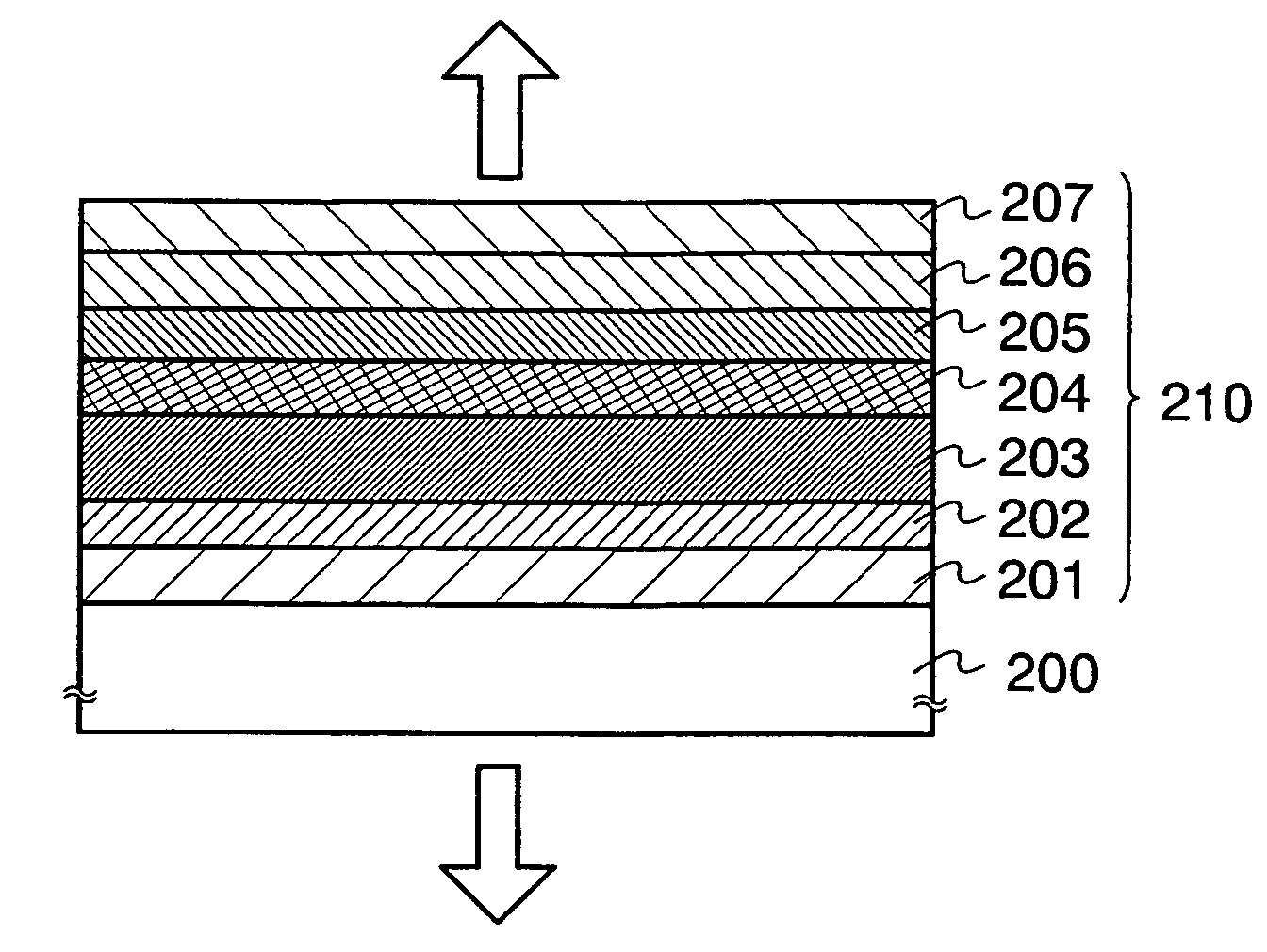
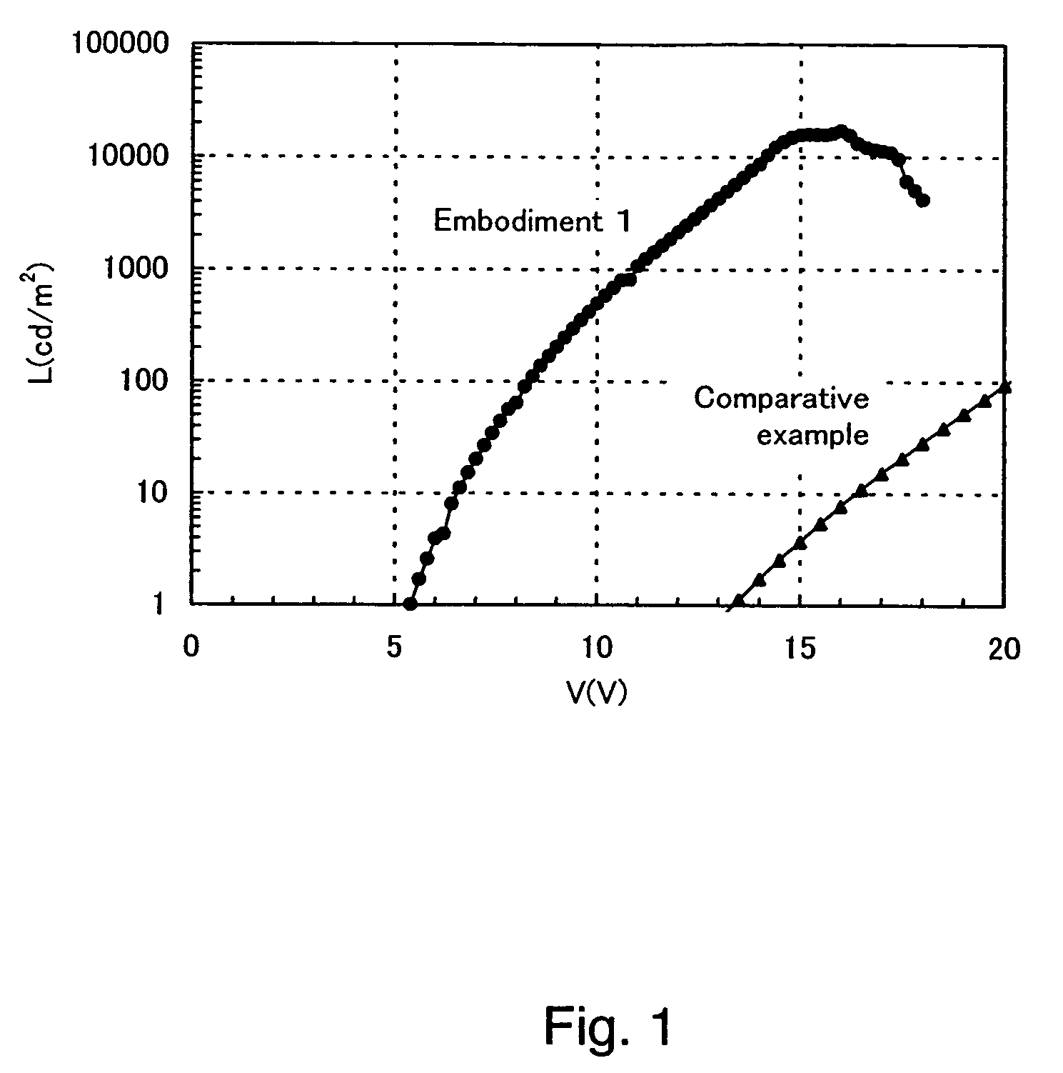
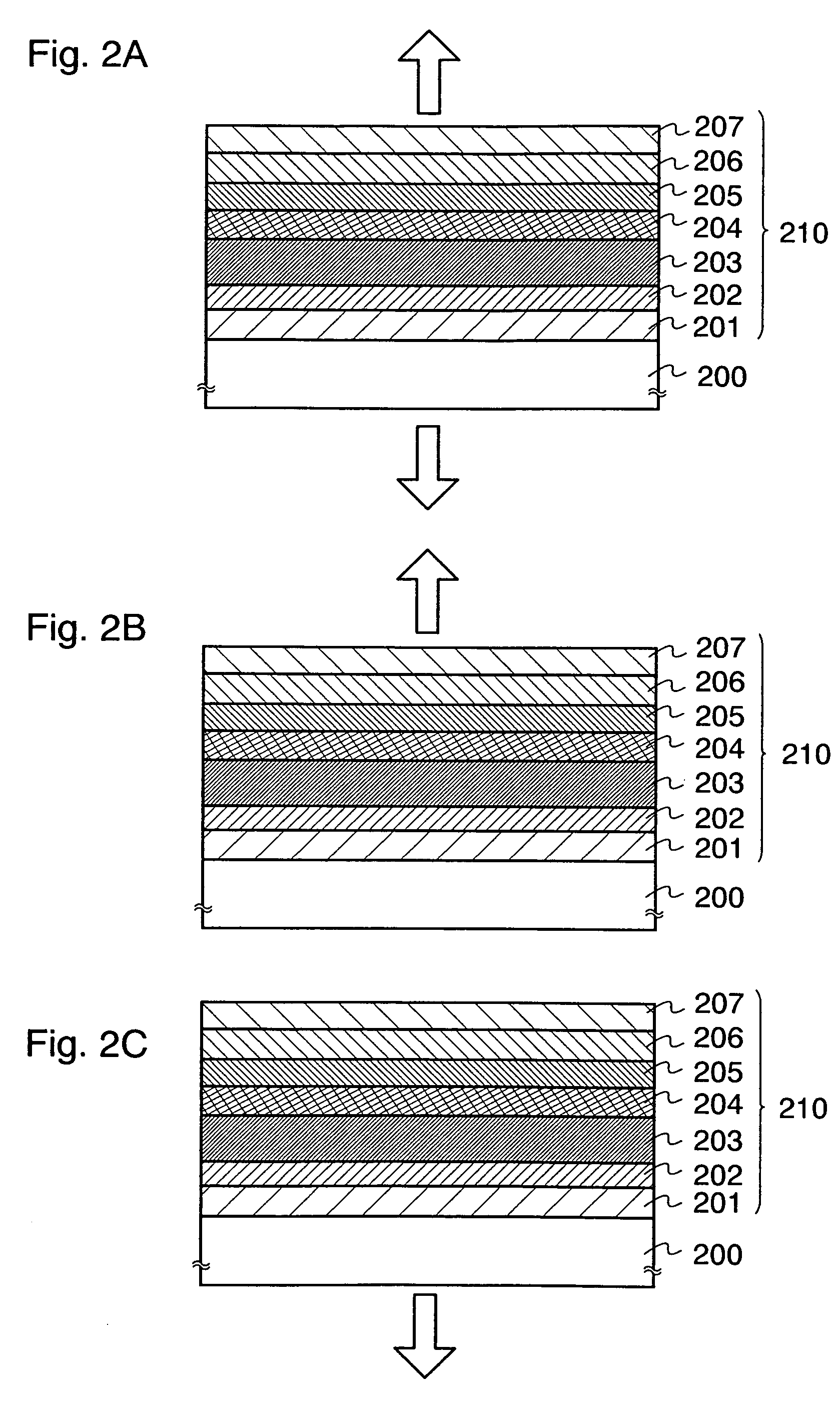
[0063]A manufacturing method of a light-emitting element according to the present invention and characteristics of the light-emitting element will be described. The structure or manufacturing process of the light-emitting element according to the present invention is not limited to the present embodiment, and a film thickness or a material, for example, may be changed appropriately.

[0064]On a glass substrate, indium tin oxide (ITO) is deposited by sputtering to form a first electrode, where ITO in the deposition contains an amorphous component as its main component. Next, after etching ITO to be separated into elements, a heat treatment is performed at 200° C. for 1 hour. Further, after applying an acrylic that is a positive type photoresist, exposure and development are performed to form a partition layer. After that, a heat treatment is performed at 220° C. for 1 hour.

[0065]Next, after wet cleaning, the glass substrate with ITO deposited is processed at 150° C. for 30 minutes in a...

embodiment 2

[0078]In the present embodiment, a light-emitting element that has the same structure as that shown in Embodiment 1 except that the fifth layer including molybdenum oxide has a different film thickness form that in Embodiment 1 will be described. A manufacturing method of the light-emitting element shown in the present embodiment is also the same as that in Embodiment 1. Therefore, descriptions of the manufacturing method are omitted.

[0079]As for the light-emitting element of the present embodiment, the fifth layer including molybdenum oxide has film thicknesses of 10 nm (Embodiment 2-1), 100 nm (Embodiment 2-2), and 200 nm (Embodiment 2-3).

[0080]Characteristics of the light-emitting elements of the present embodiment are shown in FIG. 6. FIG. 6 shows voltage-luminance characteristics, where a horizontal axis indicates a voltage (V) and a vertical axis indicates a luminance (cd / m2). FIG. 6 indicates that a driving voltage (a voltage at which a light emission of 1 cd / m2 or more is st...

embodiment 3

[0082]In the present embodiment, a structure of a light-emitting device according to the present invention will be described.

[0083]In each of FIGS. 9A to 9C, a portion surrounded by a dotted line is a transistor 11 provided for driving a light-emitting element 12. The light-emitting element 12 is formed to include a first electrode 13, a second electrode 14, and a light-emitting layer 15 interposed between these electrodes. The first electrode 13 and a drain of the transistor 11 are electrically connected to each other by a wiring 17 running through a first interlayer insulating film 16a to 16c. In addition, the light-emitting element 12 is separated by a partition layer 18 from another light-emitting element provided adjacently. A light-emitting device that has this structure according to the present invention is provided over substrate 10.

[0084]In the light-emitting device that has the structure described above, the light-emitting element 12 is a light-emitting element according t...


PUM


Abstract

A light-emitting element has a layer including an organic material between a first electrode and a second electrode, and further has a layer including a metal oxide between the second electrode and the layer including the organic material, where these electrodes and layers are laminated so that the second electrode is formed later than the first electrode. The light-emitting element is suppressed damage caused to a layer including an organic material during deposition by sputtering and a phenomenon such as short circuit between electrodes.

Description

BACKGROUND OF THE INVENTION[0001]1. Field of the Invention[0002]The present invention relates to a light-emitting element that has a structure interposing a plurality of layers between a pair of electrodes, in particular, relates to a structure of the layers.[0003]2. Description of the Related Art[0004]A light-emitting device utilizing a light emission from an electroluminescent element (a light-emitting element) has been attracting attention as a device, for example, for displaying or for lighting.[0005]As the light-emitting element that is used for the light-emitting device, an element that has a structure interposing a plurality of layers, each including a material such as a luminescent or carrier transporting material, between a pair of electrodes is well known.[0006]In the case of this light-emitting element, one of the electrodes functions as an anode while the other electrode functions as a cathode, a hole injected from the anode side and an electron injected from the cathode...

Claims


Application Information

Patent Timeline
Patent Type & Authority Patents(United States)
IPC IPC(8): H01L21/00H05B33/26H01L29/04H01L51/50H05B33/10H05B33/12H05B33/22
CPCH01L51/5092H01L51/5088H01L51/5048H01L2251/5315H10K50/14H10K50/171H10K50/17H10K50/81H10K2102/341H10K2102/3026H10K59/873H05B33/26H10K50/844H10K50/15H10K50/16H10K2102/00
Inventor SAITO, KEIKOIKEDA, HISAO
Owner SEMICON ENERGY LAB CO LTD
Learn More