Semiconductor memory device and method for fabricating the same

a memory device and semiconductor technology, applied in the direction of semiconductor devices, electrical devices, transistors, etc., can solve the problems of increasing manufacturing costs, increasing soi structure, and increasing fabrication costs, and achieve the effect of easy fabrication

Inactive Publication Date: 2006-04-20
FUJITSU LTD
View PDF14 Cites 12 Cited by
  • Summary
  • Abstract
  • Description
  • Claims
  • Application Information

AI Technical Summary

Benefits of technology

[0017] The above-described object is achieved by a semiconductor memory device comprising: a silicon layer having a first diffused region and a second diffused region formed therein; a gate electrode formed through an insulating film on one side of the silicon layer between the first and the second diffused regions; a capacitor formed on said one side of the silicon layer and having a storage electrode connected to the first diffused region; and a bit line formed on the other side of the silicon layer and connected to the second diffused region, whereby a semiconductor memory device of SOI structure can be easily fabricated.
[0018] The bit line connected to the second diffused region is formed on the other side of the semiconductor layer, whereby the bit line can be arranged without restriction by the structure, etc. of the capacitor. Short circuit between the capacitor and the bit line can be prevented.
[0019] The above-described object is also achieved by a semiconductor memory device comprising: a silicon layer having a first diffused region and a second diffused region formed therein; a gate electrode formed through an insulating film on one side of the silicon layer between the first and the second diffused regions; a capacitor formed on said one side of the silicon layer and having a storage electrode connected to the first diffused region; a bit line formed on said one side of the silicon layer and connected to the second diffused region; and a strapping word line formed on the other side of the silicon layer and connected to the gate electrode, whereby a semiconductor memory device of SOI structure can be easily fabricated.

Problems solved by technology

This is a disadvantage.
Lower electric power consumption of the device as well as higher integration has achieved, but the electric power consumption reduction makes the junction capacitance of the device more influential, which is a barrier to higher speed operation of the device.
The DRAM using the above-described conventional SOI structure can simplify the capacitor forming process to thereby decrease costs, but cost increase due to the use of the SOI structure exceeds the cost decrease, sometimes with the result of higher fabrication costs.
Because SOI substrates are usually more susceptible of heat treatments than the usual substrates, the wafers are easily deformed, and crystal defects are easily introduced.
As a result, the fabrication yields are often low.
This often adds to fabrication costs of the DRAM.
The polishing step often adds to fabrication costs.
This often adds to fabrication costs.
The use of the SOI structure makes it difficult to apply back bias to the channel regions of transistors, and the source-drain voltage resistance is often degraded due to charges accumulated in the back gates.
In the conventional DRAM structure, however, a number of lines and capacitors are formed on the bit line, which makes it difficult to cover the bit lines with the shield electrodes.
The above-described disadvantages make it difficult to form memories of high soft error immunity and reliability, which makes it accordingly difficult to reduce the capacitance to thereby simplify the fabrication process.

Method used


Image

  • Semiconductor memory device and method for fabricating the same
  • Semiconductor memory device and method for fabricating the same
  • Semiconductor memory device and method for fabricating the same

Examples


first embodiment

A FIRST EMBODIMENT

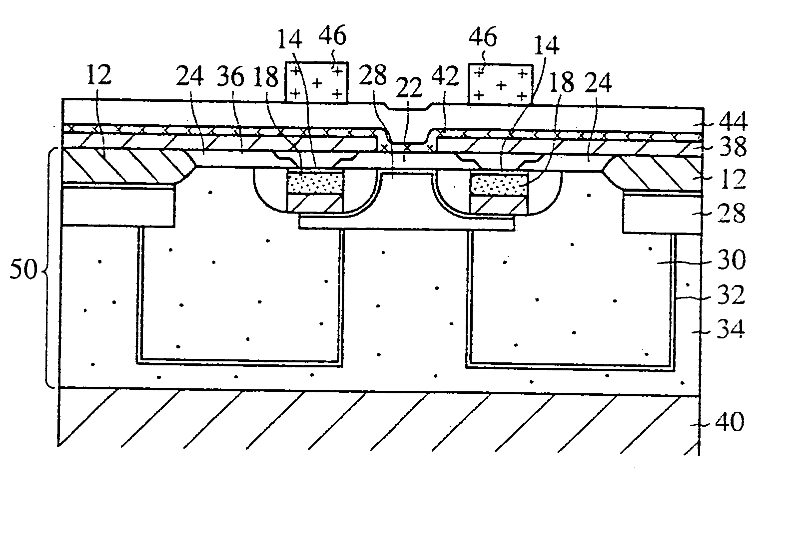
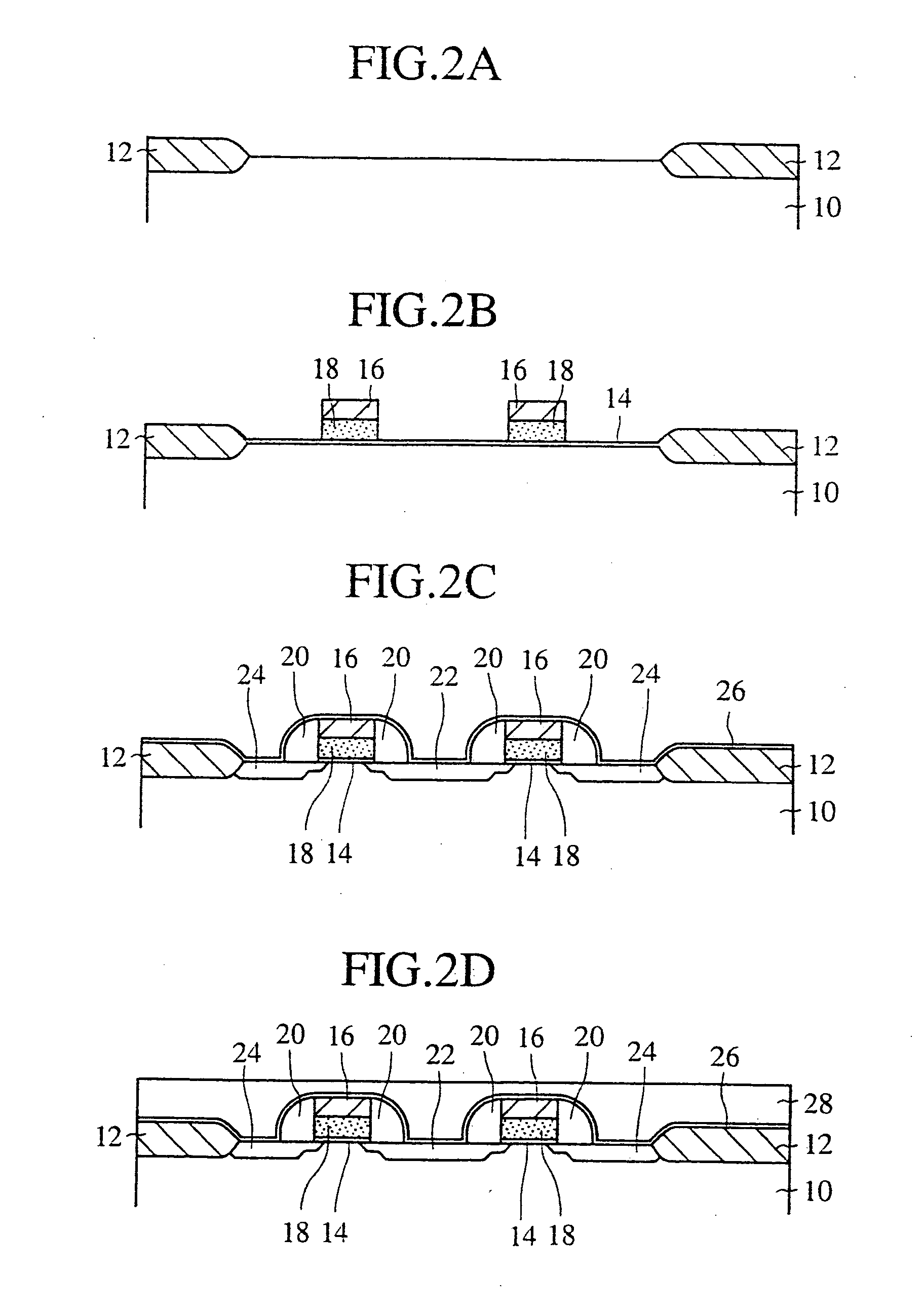
[0086] The semiconductor memory device and a method for fabricating the same according to a first embodiment of the present invention will be explained with reference to FIGS. 1 to 5.

[0087]FIG. 1 is a diagrammatic sectional view of the semiconductor memory device according to the present embodiment, which explains a structure thereof. FIGS. 2 to 5 are sectional views of the semiconductor memory device on the steps of the method for fabricating the semiconductor memory device according to the present embodiment.

[0088] First, a structure of the semiconductor memory device according to the present embodiment will be explained with reference to FIG. 1.

[0089] A device layer 50 with memory cells formed on is adhered to a support substrate 40.

[0090] A source diffused region 22 and a drain diffused region 24 are formed independent of each other in a semiconductor layer 36 formed in the device layer 50 and defined by a device isolation film 12. A gate electrode 18 to be...

second embodiment

A SECOND EMBODIMENT

[0148] The semiconductor memory device according to a second embodiment of the present invention and a method for fabricating the same will be explained with reference to FIGS. 9 to 14. The same members of the present embodiment as those of the semiconductor memory device according to the first embodiment are represented by the same reference numerals so as not to repeat or to simplify their explanation.

[0149]FIG. 9 is a diagrammatic sectional view of the semiconductor memory device according to the present embodiment, which show a structure thereof. FIGS. 10 to 23 are sectional views of the semiconductor memory device according to the present embodiment on the steps of the method for fabricating the same, which explain the method.

[0150] The semiconductor memory device according to the present embodiment is characterized in that strapping word lines 46 are formed on the side of a support substrate 40. That is, the strapping word lines 46 which decrease electric ...

third embodiment

A THIRD EMBODIMENT

[0177] The semiconductor memory device according to a third embodiment of the present invention will be explained with reference to FIGS. 14 to 18. The same members of the present embodiment as those of the semiconductor memory device according to the first and the second embodiments and the method for fabricating the same are represented by the same reference numerals so an not to repeat or to simplify their explanation.

[0178]FIG. 14 is a diagrammatic sectional view of the semiconductor memory device according to the present embodiment, which explains a structure thereof. FIGS. 15 to 18 are sectional views of the semiconductor memory device according to the present embodiment on the steps of the method for fabricating the same, which explain the method.

[0179] The semiconductor memory device according to the present embodiment is characterized in that bit lines are formed on the side of a semiconductor layer 36 on which capacitors are formed. That is, the bit lin...


PUM


Abstract

A semiconductor memory device comprises a silicon layer having a first diffused region and a second diffused region formed therein, a gate electrode formed through an insulating film on one side of the silicon layer between the first and the second diffused regions, a capacitor formed on said one side of the silicon layer and having a storage electrode connected to the first diffused region, and a bit line formed on the other side of the silicon layer and connected to the second diffused region, whereby a semiconductor memory device of SOI structure can be easily fabricated. The bit line connected to the second diffused region is formed on the other side of the semiconductor layer, whereby the bit line can be arranged without restriction by the structure, etc. of the capacitor. Short circuit between the capacitor and the bit line can be prevented.

Description

[0001] This application is a divisional of prior application Ser. No. 10 / 939,598 filed Sep. 14, 2004, which is a divisional application of prior application Ser. No. 10 / 003,304 filed Dec. 6, 2001, now U.S. Pat. No. 6,831,322, which is a divisional application of prior application Ser. No. 08 / 970,212 filed Nov. 14, 1997, now U.S. Pat. No. 6,472,703, which is a divisional application of prior application Ser. No. 08 / 660,324 filed Jun. 4, 1996, now U.S. Pat. No. 5,776,789, the benefit of which is claimed under 35 U.S.C. §120.BACKGROUND OF THE INVENTION [0002] The present invention relates to a semiconductor memory device, more specifically to a semiconductor memory device and a method for fabricating the same which can fabricate a DRAM (Dynamic Random Access Memory) of high integration and high efficiency at low costs. [0003] A DRAM is a semiconductor device which may comprise one transistor and one capacitor, and its structures and methods for fabricating the structures have been conv...

Claims


Application Information

Patent Timeline
Patent Type & Authority Applications(United States)
IPC IPC(8): H01L21/8242H01L21/84H01L27/108H01L27/12
CPCH01L21/84H01L27/108H01L27/1082H01L27/10844H01L27/10873H01L27/1203H01L29/945H10B12/33H10B12/01H10B12/00H10B12/05
Inventor NAKAMURA, SHUNJI
Owner FUJITSU LTD
Why Eureka
Try Eureka