
Forming transparent crystalline elements by cold working

a technology of transparent crystals and cold working, which is applied in the field of cold working preparation of optical elements for infrared applications, can solve the problems of complex process, high cost, time-consuming and expensive, etc., and achieve the effect of low cost and high sensitivity

Inactive Publication Date: 2008-06-10
KATZIR ABRAHAM
View PDF4 Cites 2 Cited by
  • Summary
  • Abstract
  • Description
  • Claims
  • Application Information

AI Technical Summary

Benefits of technology

[0053]According to a preferred embodiment of the present invention, the IR elements are formed of halide salts that are relatively soft and ductile (i.e., elongation ratio greater than about 10%), for example silver halides and thallium halides. Halides, such as AgClBr exhibit a mechanical behavior that is somewhat similar to copper. Therefore the hardness of the optical elements may be changed: they may be made harder, due to work hardening, or softer, due to an annealing process. The annealing is useful during the steps of press forming of the IR elements. The hardening generates optical elements that are much easier to use than the softer single crystals themselves.
[0057]The present invention solves the problem of using cold working for making infrared elements, without causing cracks and without causing darkening in the forged pieces. This method lends itself to mass production of inexpensive infrared elements.
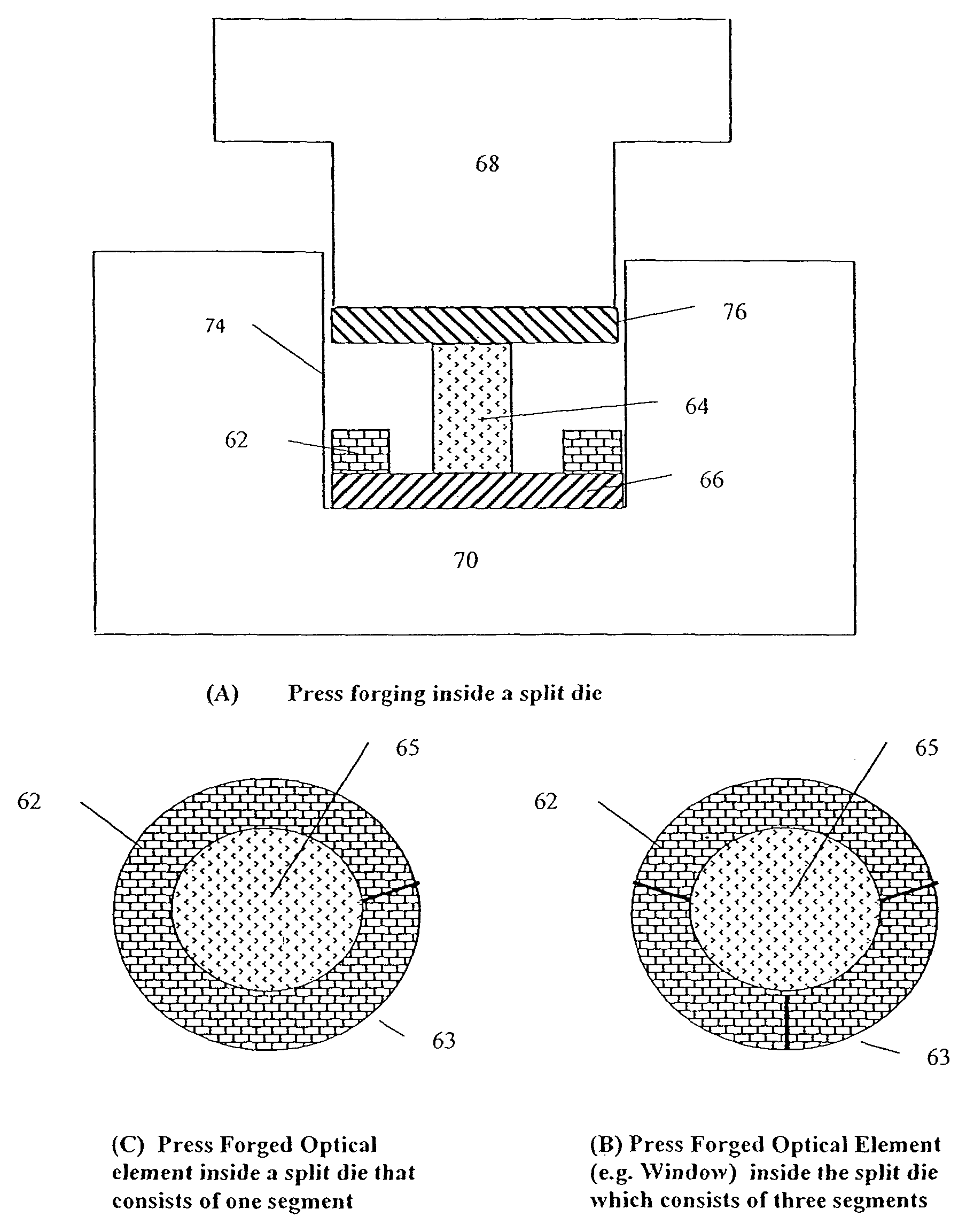
[0058]According to the present invention, there is provided a simple and inexpensive way of producing both “bulk” ATR elements and thin waveguide elements for evanescent wave spectroscopy. The “bulk” elements are formed by mechanical deformation of IR transmitting crystalline materials inside a sacrificial die. Thin planar waveguides also may be formed in the same way but preferably are formed by the press forging of flexible IR fibers.
[0064]Further, according to another preferred embodiment of the present invention, the plate merges into ends of greater thickness, for coupling in light. The present invention successfully addresses the shortcomings of the presently known fiberoptic configurations by providing a flat optical waveguide which is inexpensive to manufacture, which can be formed to any desired length, which has a relatively large surface area contacting the sample, which is sufficiently flexible to conform to a wide variety of samples and which provides straightforward and accurate measurements of attenuated total reflection. In particular, use of these waveguides does not require complex calculations of angle of incidence and so forth. It has been shown both theoretically and experimentally that the use of thin waveguides will tremendously increase the sensitivity of diagnostic systems.
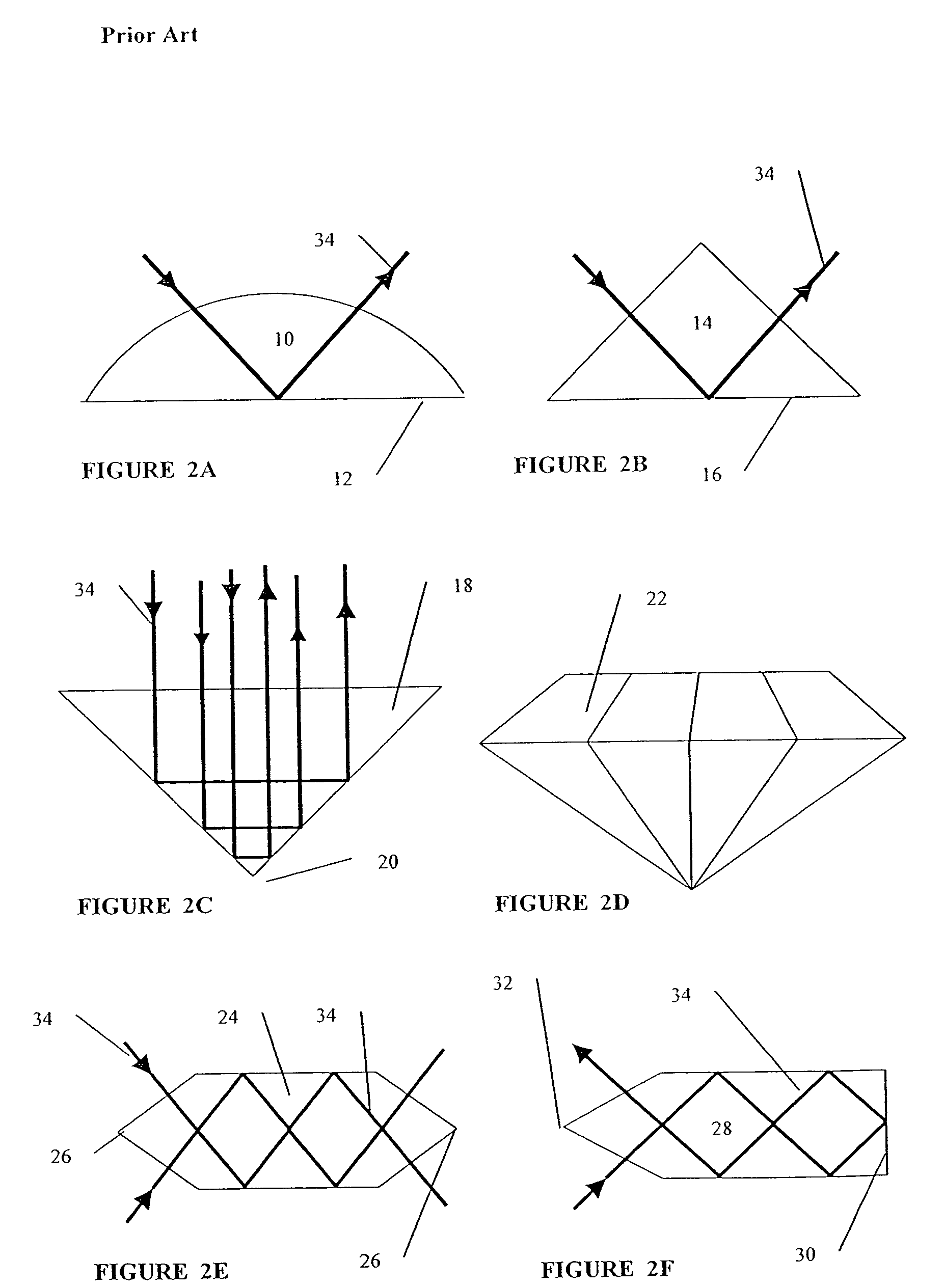
[0071]In all the above-mentioned applications, it is advantageous to use ATR elements that are fabricated by cold working, because of their low cost. These could be part of a regular infrared spectrometer or part of a FEWS system. If high sensitivity is desirable, then the thin flat waveguides discussed above and tunable IR lasers should be used.

Problems solved by technology

This has been used mostly for military applications (e.g. FLIR), because the arrays used were very expensive.
In many of these cases the process is much more complicated than for silica, because many of the IR materials are difficult to handle: they are brittle, water soluble or toxic.
In all cases the process of making IR optical elements is complicated, time consuming and expensive, especially when trying to make large optical elements.
Some of these processes have been adapted for the fabrication of diffractive optics IR elements, notably by the Coherent Auburn Group of Auburn Calif., but the processes are time consuming and rather expensive.
If the extra hardening is undesirable, annealing at elevated temperatures can soften the bodies.
Unfortunately almost all of these crystals are hard and brittle and much less ductile than metals and it is difficult to deform them without fracture.
Apparently there are technical hurdles that have not yet been surmounted.
Inexpensive, mass produced, infrared elements made of any of the materials mentioned above are not available in large quantities.
The optical transmission of these fibers is still not satisfactory, and they are not widely used.
None of these lenses is available commercially, and they have not been discussed in the scientific literature.
Summarizing this prior art, one may conclude that the three methods mentioned above cannot be used for mass production of infrared transmitting optical elements of high quality.
The rolling technique described in (I) can be used only for making thin flat sheets, and the optical quality of the sheets obtained was rather poor.
In extensive work done by us, we discovered great disadvantages of this forging method.
When one tries to forge elements at relatively low temperature (below 120° C.) the lenses crack.
This causes two problems: (i) the optical elements darken and their transmission is very poor.
(ii) the walls of the chamber gradually deteriorate and become useless.
It is possible to protect the top and bottom pressure plates by a thin layer of carbon or non-reactive metal, but it is not possible to protect the sidewalls.
It is not practical to replace the very expensive pressure chamber after every forging procedure.
(1) almost all these studies referred to single crystals or polycrystalline samples of AgCl or AgBr and not to alloys, such as AgClBr; (2) in most cases, the samples contained impurities in concentrations higher than 10 ppm; (3) most of the samples were photosensitive: they darkened under UV or visible light. All these ductile halide crystals are potentially suited for the fabrication of a plethora of infrared elements by the well-established metallurgical cold working methods. They have not been widely used, only because of the severe problems mentioned above.
(IV) Forge pressing at a well defined temperature range 120-180° C. As mentioned, forge pressing at lower temperatures gives rise to cracks in the optical elements (especially in the case of large elements), and forge pressing at higher temperature gives rise to darkening.
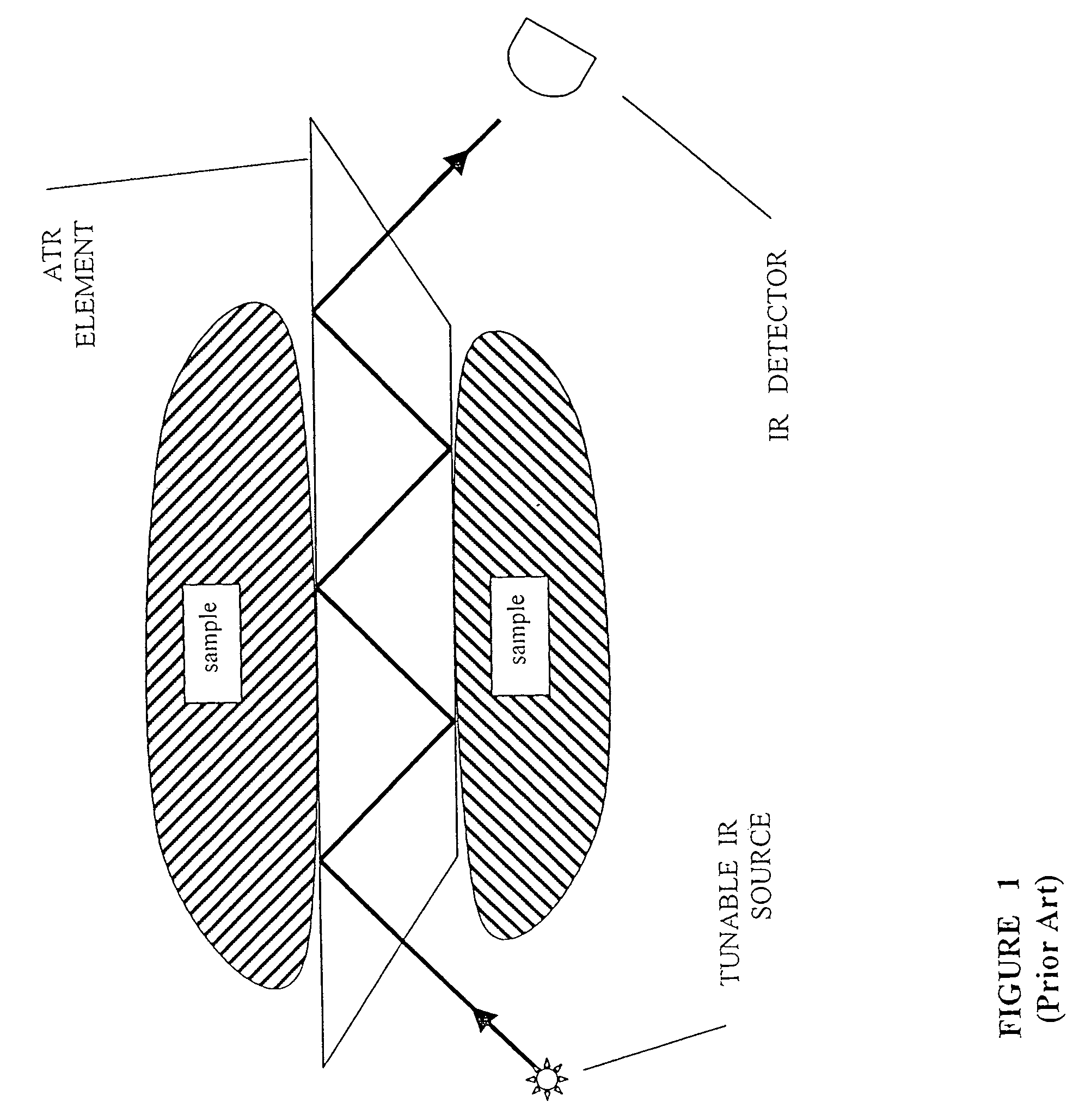
ATR spectroscopy has been widely used for the study of IR spectra of samples, which are not easy to measure by conventional transmission techniques.
However, the “bulk” elements are large, expensive and susceptible to damage, because of mechanical scratches and because of chemical interaction with the measured samples.
Furthermore, these elements are not flexible and they require frequent polishing to maintain their useful qualities.
However, even these cylindrical fibers are not ideal as sensing elements.
While they overcome the problems of difficulty of working, they are still problematic with regard to the angle of incidence.
Optimum configurations must be found since the signal-to-noise ratio increases as the fiber diameter decreases, while if the diameter is very small, it is difficult to couple light into the fiber.
Very small pieces of chalcogenide glass fiber (2.5 cm long and 400 microns in diameter) were tried, but did not have adequate sensitivity.
ymer. Solute molecules (e.g. pollutants in water) can diffuse in, but the solvent (e.g. water) c
There are, however, a number of disadvantages in the use of these tapered fibers.
First, due to their cylindrical cross-section, a unique angle of incidence cannot be maintained, so calibrations and calculations are necessary when they are used.
Second, chalcogenide glasses can be difficult to work with, because of their brittleness and the small area of contact between the tapered (cylindrical) sensor and the sample.
This has proven to be much more difficult than had been anticipated.
There are still severe obstacles in using modern optical methods for tissue diagnosis or blood analysis.
Still, IR spectroscopic methods, including FTIR—ATR spectroscopy of tissues and biological fluids, have not yet gained acceptance among physicians.
The methods used rely on scattering of light or on determining the color of the skin, but, again, these methods are limited (U.S. Pat. Nos. 4,494,869, 5,094,248 and 5,745,217).

Method used


Image

  • Forming transparent crystalline elements by cold working
  • Forming transparent crystalline elements by cold working
  • Forming transparent crystalline elements by cold working

Examples


Embodiment Construction

[0097]The present invention is of a method of preparing a monocrystalline or polycrystalline ingot of a soft and ductile IR-transmissive material and cold working the ingot to produce polycrystalline elements of desired shapes. Specifically, the present invention can be used to make optical elements for ATR infrared spectroscopy.

[0098]The principles and operation of producing IR optical elements according to the present invention may be better understood with reference to the drawings and the accompanying description.

[0099]The mechanical methods used in the present invention are similar to the cold working methods used in metallurgy. These include press forging for the fabrication of “bulk” optical elements and stamping, or coining, or embossing, for the fabrication of “surface” optical elements.

[0100]The preferred starting material is a large crystal that is highly transparent in the mid-infrared and is ductile. The crystal is of very high purity, and with minimum scattering. The r...


PUM

PropertyMeasurementUnit
temperatureaaaaaaaaaa

Abstract

An infrared optical element, and methods for its manufacture. The optical element is made by cold working an ingot of a soft crystalline ionic solid such as silver halide or a thallium halide inside a sacrificial split die. The solid preferably includes at most one part per million of metallic impurities and at most ten parts per million total impurities. Preferably, the Knoop hardness of the ionic solid is at most about 20, and the elongation ratio of the ionic solid is at least 10% at a temperature of 120-180° C. The optical element maybe a bulk element or a surface element. The optical element may be a refractive element, a diffractive element or a hybrid element. One such element is a flat sensor for attenuated total reflection spectroscopy. In one embodiment of the sensor, a thin layer of silver halide or thallium halide is formed by diffusion or deposition on the surface of a substrate having a lower index of refraction than the layer. The sensor also includes a mechanism for coupling infrared radiation in and out of the layer. The scope of the invention includes a cell for attenuated total reflection spectroscopy based on the sensor, and a spectrometer for attenuated total reflection spectroscopy based on the cell. It also includes an external sensor, which is connected to the spectrometer via two long infrared fibers, which enable measurements in remote locations.

Description

[0001]This is a Continuation-in-Part of U.S. patent application Ser. No. 10 / 138,581 filed May 6, 2002, now abandoned, which is a Continuation of U.S. patent application Ser. No. 09 / 458,688 filed Dec. 10, 1999, now abandoned, which is based on U.S. Provisional Application No. 60 / 111,929 filed Dec. 11, 1998.FIELD AND BACKGROUND OF THE INVENTION[0002]The present invention relates to the preparation of optical elements by cold working of formable (i.e. ductile) crystals. More specifically, the present invention relates to the preparation of elements for infrared applications, using processes such as cold forging, embossing, or stamping, which are carried out in a narrow temperature range, using a sacrificial split die. The present invention also relates to the use of such elements, and in particular of thin waveguides, as the bases for a system that can be applied for the diagnosis of tissues or biological fluids, in medicine. The same diagnostic system could be used in cosmetics for sk...

Claims


Application Information

Patent Timeline
Patent Type & Authority Patents(United States)
IPC IPC(8): G02B1/00B28B5/00G01N21/55G02B6/12G02B6/122G02B6/34
CPCG01N21/552G02B6/122G02B6/34G02B2006/12102G02B2006/12107
Inventor KATZIR, ABRAHAM
Owner KATZIR ABRAHAM
Learn More