GMR magnetic sensing element having an antiferromagnetic layer extending beyond the track width and method for making the same
a magnetic sensing element and antiferromagnetic layer technology, applied in the field of magnetic sensing elements, can solve the problems of reducing the quality of the magnetic sensing element, difficult to remove the resist layer rb>1/b>, and reducing the magnetic detection outpu
- Summary
- Abstract
- Description
- Claims
- Application Information
AI Technical Summary
Benefits of technology
Problems solved by technology
Method used
Image
Examples
first embodiment
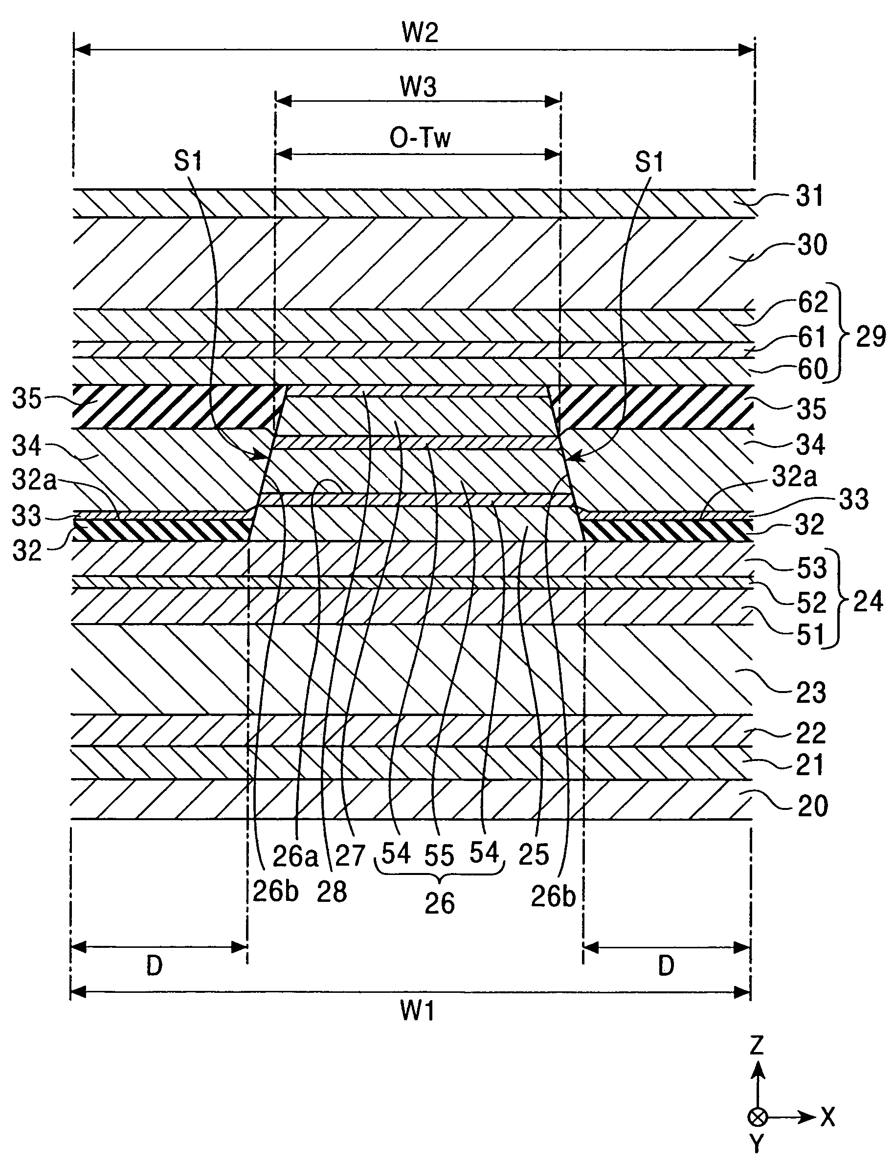
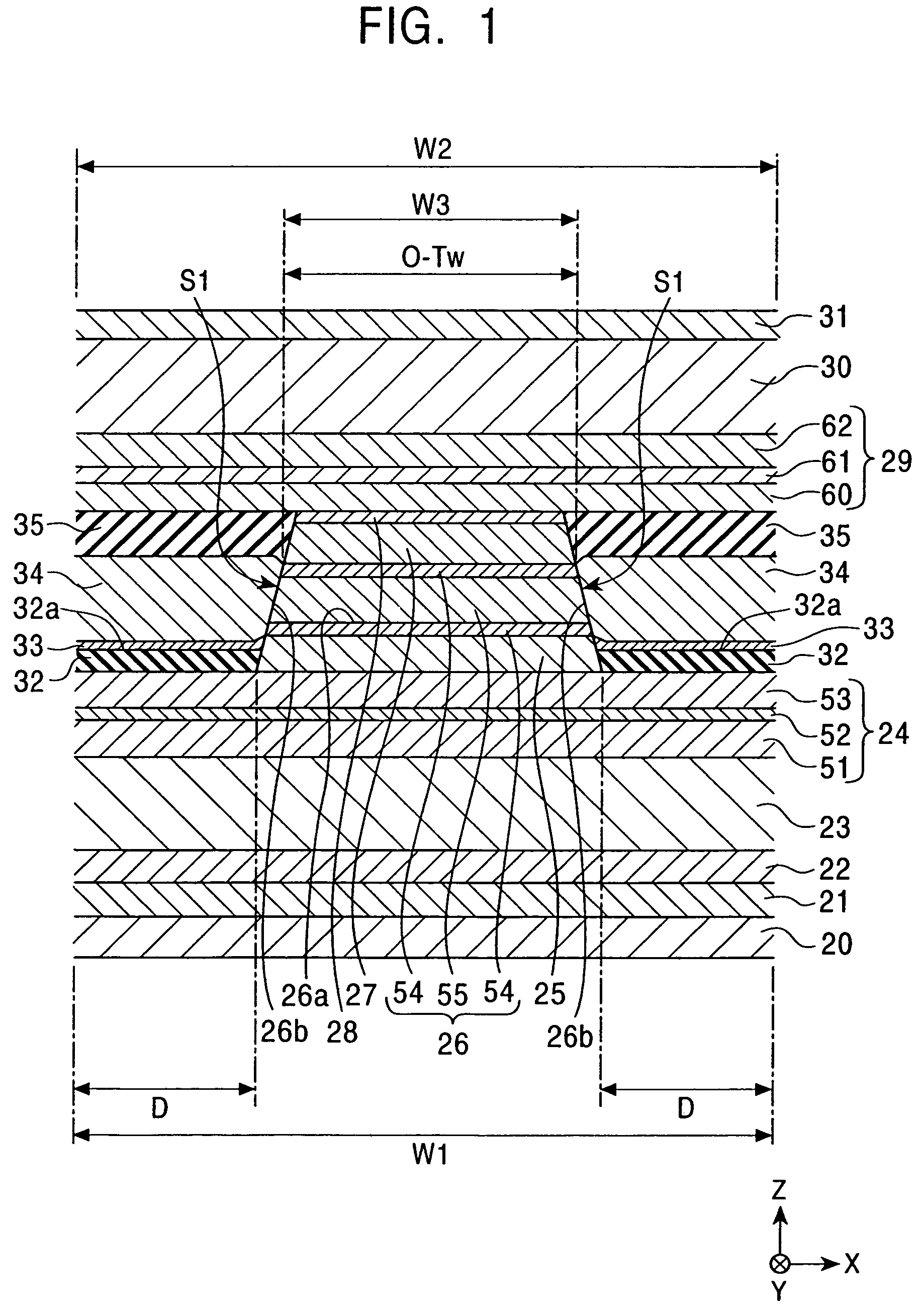
[0105]FIG. 1 is a cross-sectional view showing an overall structure of a magnetic sensing element according to a first embodiment of the present invention viewed from the opposing face. The magnetic sensing element is of a dual spin-valve type.
[0106]The magnetic sensing element includes a first electrode layer 20 composed of, for example, α-Ta, Au, Cr, Cu, or W.
[0107]An underlayer 21 is formed on the upper face of the first electrode layer 20. The underlayer 21 is preferably composed of at least one of Ta, Hf, Nb, Zr, Ti, Mo and W. The thickness of the underlayer 21 is 50 Å or less. Alternatively, no underlayer 21 may be formed.
[0108]A seed layer 22 is disposed on the underlayer 21. The seed layer 22 is mainly face-centered cubic and has the (111) faces preferentially oriented in a direction parallel to the interface with a lower antiferromagnetic layer 23 described below. The seed layer 22 is preferably composed of elemental Cr, a NiFe alloy, or a Ni—Fe—Y alloy wherein Y is at leas...
second embodiment
[0188]FIG. 4 is a cross sectional view showing the overall structure of a dual spin-valve magnetic sensing element according to a second embodiment of the present invention viewed from the opposing face.
[0189]The magnetic sensing element shown in FIG. 4 differs from the magnetic sensing element shown in FIG. 1 in that the current limiting layer 28 is formed within an upper nonmagnetic material layer 70.
[0190]The upper nonmagnetic material layer 70 is constituted from a lower sublayer 71 and an upper sublayer (second nonmagnetic material layer) 72. The two side faces of the lower sublayer 71 are flush with the two side faces of the free magnetic layer 26 and the two side faces of the current limiting layer 28. The two side faces of the upper sublayer 72 are flush with the two side faces of the upper pinned magnetic layer 29 and the two side faces of the upper antiferromagnetic layer 30. The lower sublayer 71 and the upper sublayer 72 are both composed of copper.
[0191]The current limi...
third embodiment
[0194]FIG. 5 is a cross-sectional view showing the overall structure of a magnetic sensing element according to a third embodiment of the present invention viewed from the opposing face.
[0195]The magnetic sensing element shown in FIG. 5 includes a Ta underlayer 80 formed on the first electrode layer 20, a free magnetic layer 81, a nonmagnetic material layer 82, a current limiting layer 83, a pinned magnetic layer 84, an antiferromagnetic layer 85, and the second electrode layer 31, sequentially stacked on the underlayer 80.
[0196]The first electrode layer 20 and the second electrode layer 31 are composed of the same material and have the same thickness as those of the first electrode layer 20 and the second electrode layer 31 shown in FIG. 1.
[0197]The underlayer 80 controls the crystal orientation of the free magnetic layer 81 to improve the magnetic characteristics and to reduce the resistivity of the free magnetic layer 81.
[0198]In FIG. 5, the free magnetic layer 81 is a single mag...
PUM
| Property | Measurement | Unit |
|---|---|---|
| hard | aaaaa | aaaaa |
| hard | aaaaa | aaaaa |
| hard | aaaaa | aaaaa |
Abstract
Description
Claims
Application Information
 - R&D
- Intellectual Property
- Life Sciences
- Materials
- Tech Scout
- Unparalleled Data Quality
- Higher Quality Content
- 60% Fewer Hallucinations
Browse by: Latest US Patents, China's latest patents, Technical Efficacy Thesaurus, Application Domain, Technology Topic, Popular Technical Reports.
© 2025 PatSnap. All rights reserved.Legal|Privacy policy|Modern Slavery Act Transparency Statement|Sitemap|About US| Contact US: help@patsnap.com


