
Multiple layer resist scheme implementing etch recipe particular to each layer

a multi-layer resist and recipe technology, applied in the field of photoresist schemes, can solve the problems of difficult to achieve with current single-layer resist schemes, conventional single-layer resist schemes do not provide the mechanisms necessary to achieve the required critical dimensions, and achieve accurate cd formation. , the effect of adequate resist budg

Inactive Publication Date: 2008-04-01
TAIWAN SEMICON MFG CO LTD +2
View PDF21 Cites 6 Cited by
  • Summary
  • Abstract
  • Description
  • Claims
  • Application Information

AI Technical Summary

Benefits of technology

The invention provides methods for forming metal lines and vias in a semiconductor device using a multiple layer resist scheme. The method includes patterning a third layer of a third type material for the metal line and via critical dimension, and then sequentially etching to form the metal line and via using different tailored etch recipes for each layer. The invention provides accurate CD formation and adequate resist budget. The resist scheme includes a first layer of a first type material, a second layer of a second type material, and a third layer of a third type material. The invention allows for the formation of metal lines and vias in a single or dual damascene process on a semiconductor substrate.

Problems solved by technology

In the semiconductor industry, achieving critical dimensions on structure is a continuing challenge as devices become smaller.
One particular area that presents significant challenges relates to thin-wire line level (single) damascene processing of hydrogenated silicon oxy-carbide (SiCOH) based films for 90 nm and beyond technologies.
More particularly, conventional single layer resist schemes do not provide the mechanisms necessary to achieve the required critical dimensions.
Furthermore, current technology has desirable feature profiles such as 90° sidewalls, negligible hardmask faceting, and target line heights, which are difficult to achieve with current single layer resist schemes.

Method used


Image

  • Multiple layer resist scheme implementing etch recipe particular to each layer
  • Multiple layer resist scheme implementing etch recipe particular to each layer
  • Multiple layer resist scheme implementing etch recipe particular to each layer

Examples


Embodiment Construction

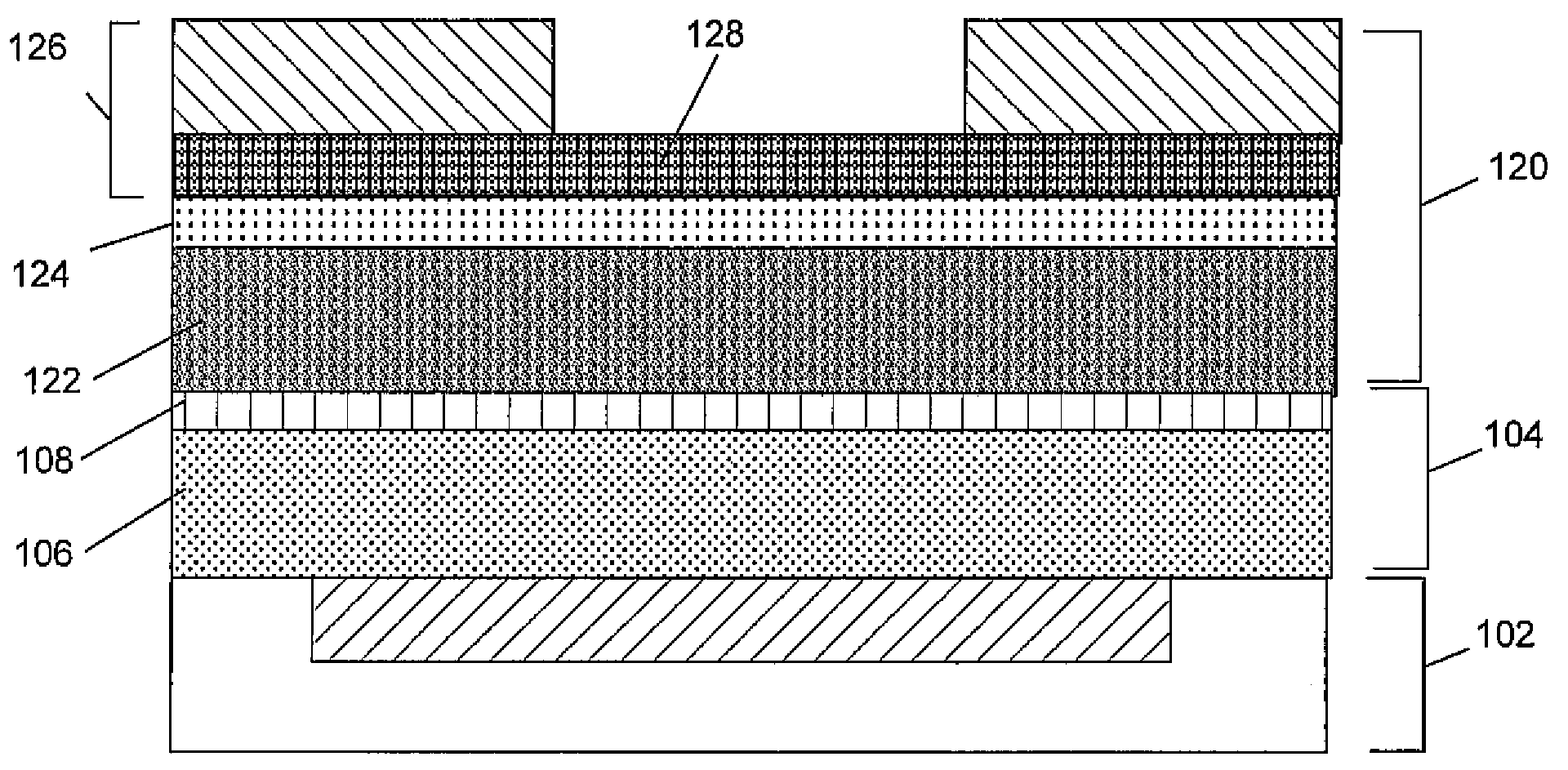
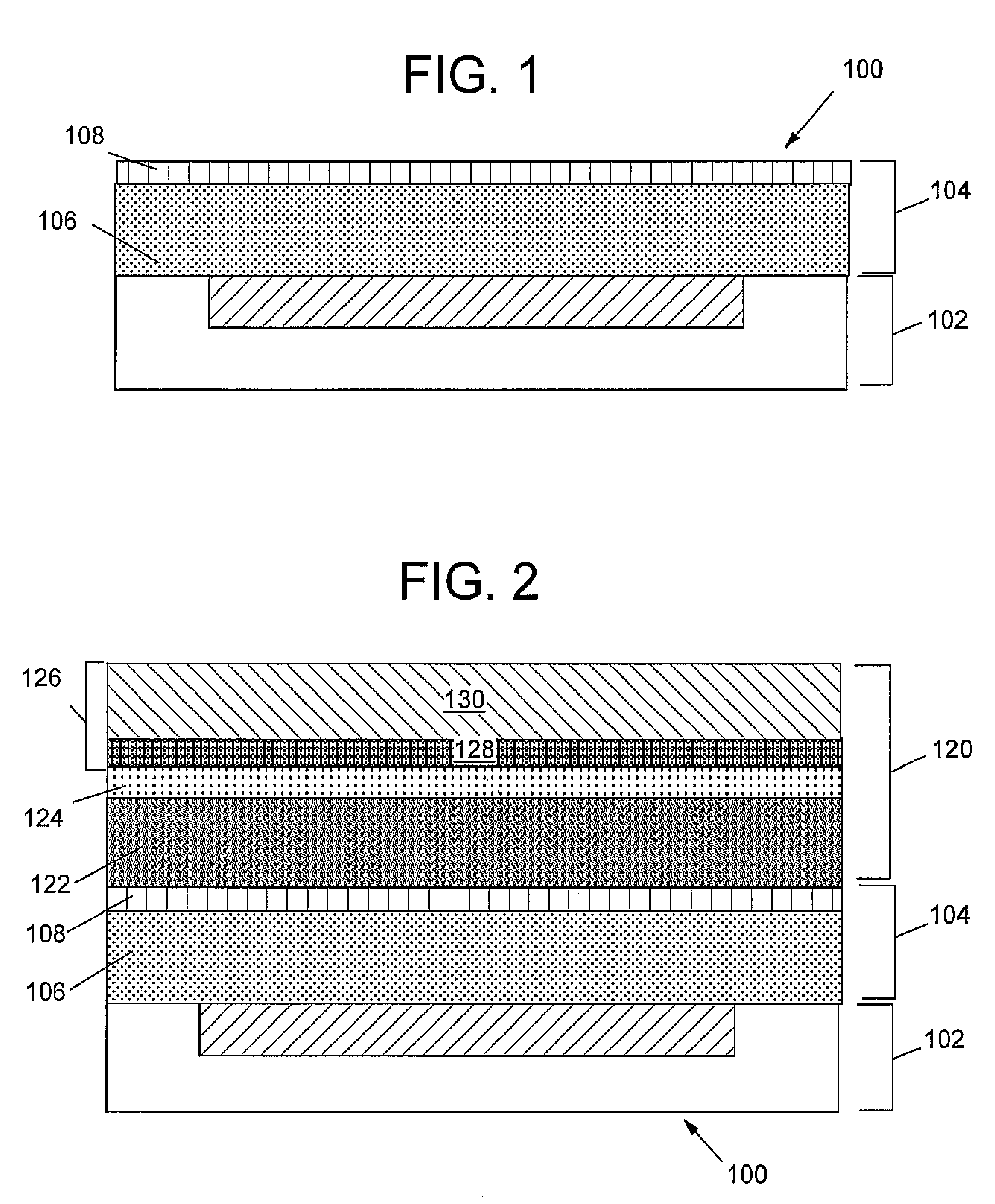
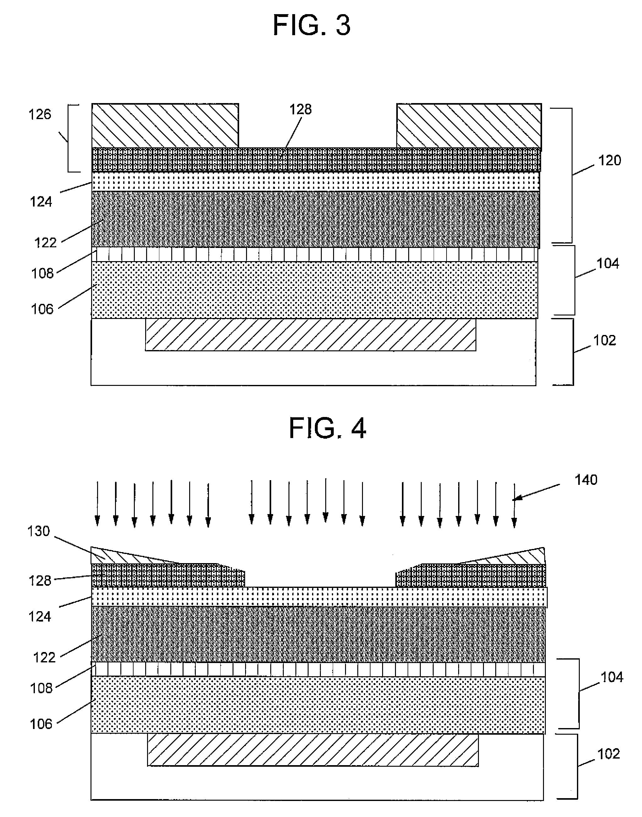
[0014]With reference to the accompanying drawings, FIG. 1 shows an initial step of a method according to one embodiment of the invention. In this embodiment, a metal line critical dimension (CD) is formed in a single damascene process on a semiconductor substrate 100. As illustrated, semiconductor substrate 100 is provided including at least one metal level 102 and at least one substrate dielectric layer 104 thereover. In one embodiment, substrate dielectric layer 104 includes two layers including a hydrogenated silicon oxy-carbide (SiCOH) layer 106 over metal level 102 and a hardmask layer 108, e.g., of oxide such as tetraethyl orthosilicate, Si(OC2H5)4 (TEOS), silicon dioxide (SiO2), silane oxide and thermal oxide. Other substrate dielectric layers such as silicon nitride (Si3N4) or silicon oxynitride (SiON) 102 may also be provided

[0015]FIG. 2 shows a next step in which a multiple layer resist scheme 120 is formed. In one embodiment, multiple layer resist scheme 120 includes a tr...


PUM


Abstract

Methods of forming a metal line and / or via critical dimension (CD) in a single or dual damascene process on a semiconductor substrate, and the resist scheme implemented, are disclosed. The method includes forming a multiple layer resist scheme including a first planarizing layer of a first type material over the substrate, a second dielectric layer of a second type material over the planarizing layer, and a third photoresist layer of a third type material over the dielectric layer. The types of material alternate between organic and inorganic material. The third layer is patterned for the metal line and / or via CD. Sequential etching to form the metal line and / or via critical dimension using a tailored etch recipe particular to each of the first photoresist layer, the second dielectric layer and the third planarizing layer as each layer is exposed is then used. Accurate CD formation and adequate resist budget are provided.

Description

BACKGROUND OF THE INVENTION[0001]1. Technical Field[0002]The present invention relates generally to photoresist schemes for semiconductor device fabrication, and more particularly, to a multiple layer resist scheme using etch recipes particular to each layer.[0003]2. Related Art[0004]In the semiconductor industry, achieving critical dimensions on structure is a continuing challenge as devices become smaller. One particular area that presents significant challenges relates to thin-wire line level (single) damascene processing of hydrogenated silicon oxy-carbide (SiCOH) based films for 90 nm and beyond technologies. More particularly, conventional single layer resist schemes do not provide the mechanisms necessary to achieve the required critical dimensions. For example, current technology may require target final critical dimension (FCD) values of 115 nm and 140 nm for the metal 1 (Ml) level and the Mx+1 levels (x=1 to 5), respectively. Furthermore, current technology has desirable f...

Claims


Application Information

Patent Timeline
Patent Type & Authority Patents(United States)
IPC IPC(8): H01L23/48H01L21/4763H01L23/52H01L29/40
CPCH01L21/0332H01L21/31138H01L21/31144H01L21/76802
Inventor FULLER, NICHOLAS C. M.DALTON, TIMOTHY J.JOY, RAYMONDLIN, YI-HSIUNGLOW, CHUN HUI
Owner TAIWAN SEMICON MFG CO LTD
Learn More