
Optical waveguide having specular surface formed by laser beam machining

a technology of laser beam machining and optical waveguide, which is applied in the direction of optical waveguide light guide, optical waveguide, instruments, etc., can solve the problems of inability to form the optical waveguide to be smaller than a predetermined size or length, and achieve the effect of reducing the size of the optical waveguide, reducing the degree of freedom in designing the optical circuit, and large divergence angl

Inactive Publication Date: 2008-01-29
MITSUI CHEM INC
View PDF26 Cites 40 Cited by
  • Summary
  • Abstract
  • Description
  • Claims
  • Application Information

AI Technical Summary

Benefits of technology

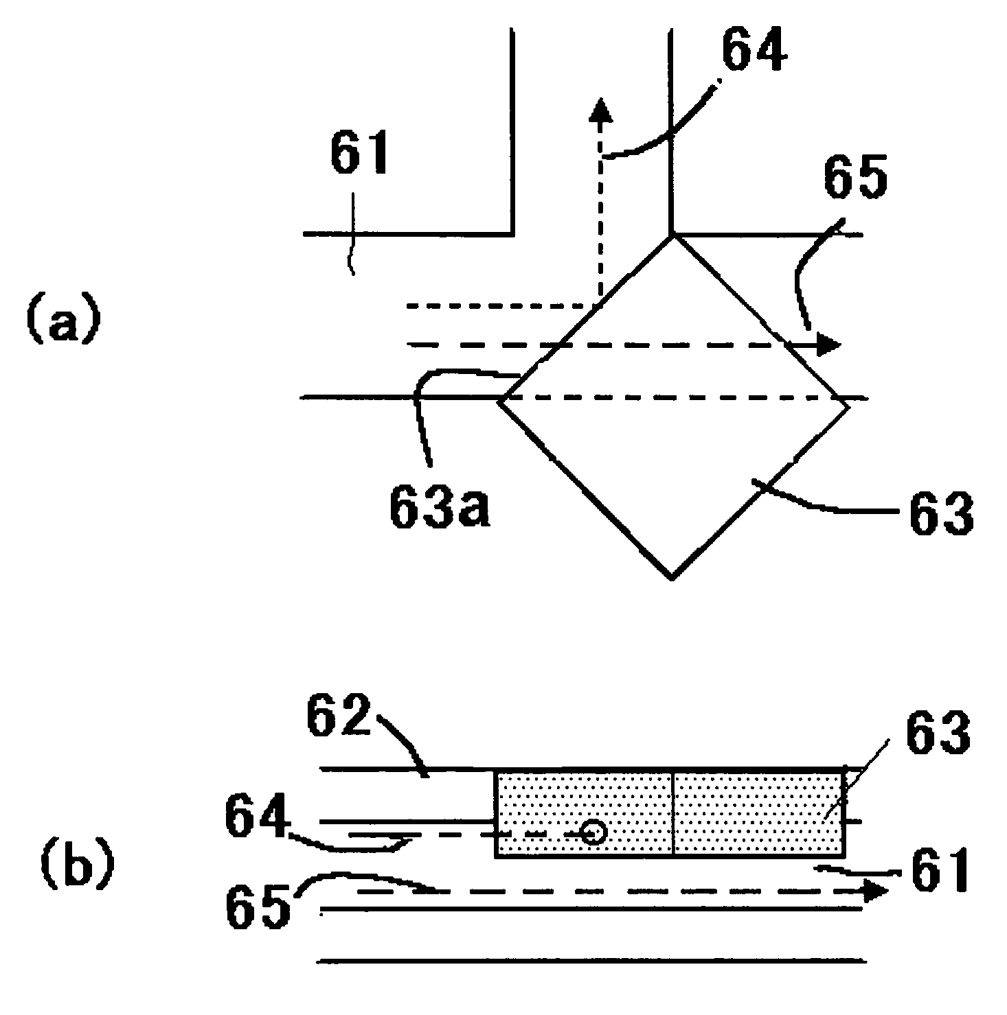
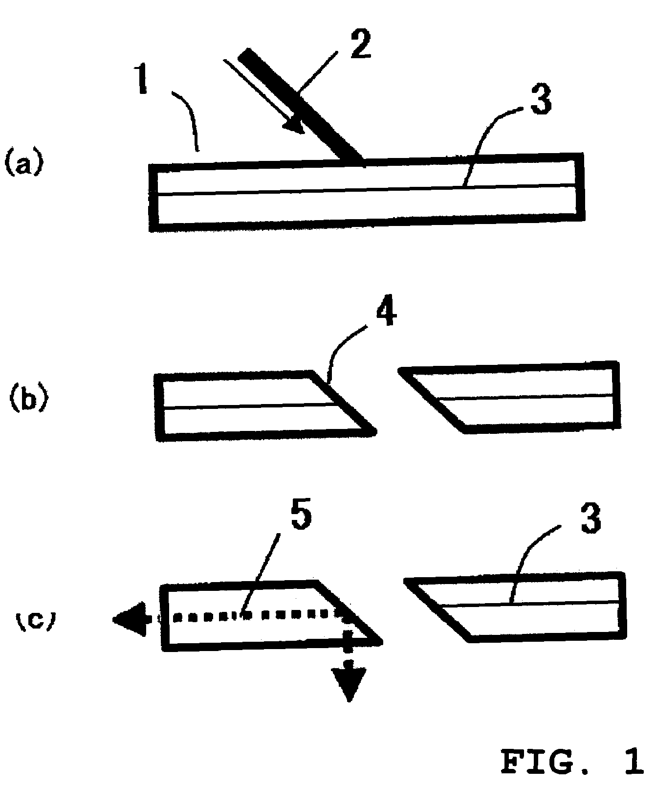
The present invention provides an optical waveguide with high efficiency optical coupling at a predetermined position in an optical circuit substrate. The optical waveguide has a core and a cladding layer, with a wall surface that is a curved specular surface. The laser beam irradiation is perpendicular to the optical waveguide plane, and the specular surface is inclined with respect to the core. This allows for optical path change at a steep angle in the optical waveguide, without the need for a micro mirror. The optical waveguide can be designed with various core patterns, and the size of the optical waveguide can be reduced. The invention also provides a method for manufacturing the optical waveguide. The technical effects of the invention include improved optical coupling, increased design flexibility, and reduced size of the optical waveguide.

Problems solved by technology

However, when using the dicing saw, even unnecessary portions are cut out at 45°.
However, in the conventional curved optical waveguide or light coupling and splitting optical waveguide, it is impossible to form the optical waveguide to be smaller than a predetermined size or length due to restriction of a specific refractive-index difference.

Method used


Image

  • Optical waveguide having specular surface formed by laser beam machining
  • Optical waveguide having specular surface formed by laser beam machining
  • Optical waveguide having specular surface formed by laser beam machining

Examples


first embodiment

[0047]Polyimide including 2,2-bis(3,4-dicarboxy phenyl) hexafluoropropane 2 anhydride (6FDA) and 2,2-bis(trifluoro methyl)-4,4′-diaminobiphenyl (TFDB) is formed as upper and lower cladding layers on a 5-inch silicon wafer, and polyimide including 6FDA and 4,4′-oxydianiline (ODA) is formed as a core layer disposed between the upper and lower cladding layers. The core on the lower cladding layer is patterned using well-known methods of photolithography and dry etching, and then the upper cladding layer is formed, thereby forming a film-shaped optical waveguide. Here, a plurality of core layers parallel to each other in the longitudinal direction is formed, thereby providing a multi array optical waveguide. Thereafter, the silicon wafer in which the optical waveguide is formed is immersed in an aqueous solution including 5 wt % of hydrofluoric acid and thus the optical waveguide is separated from the silicon wafer, thereby manufacturing a film-shaped optical waveguide. The thickness of...

second embodiment

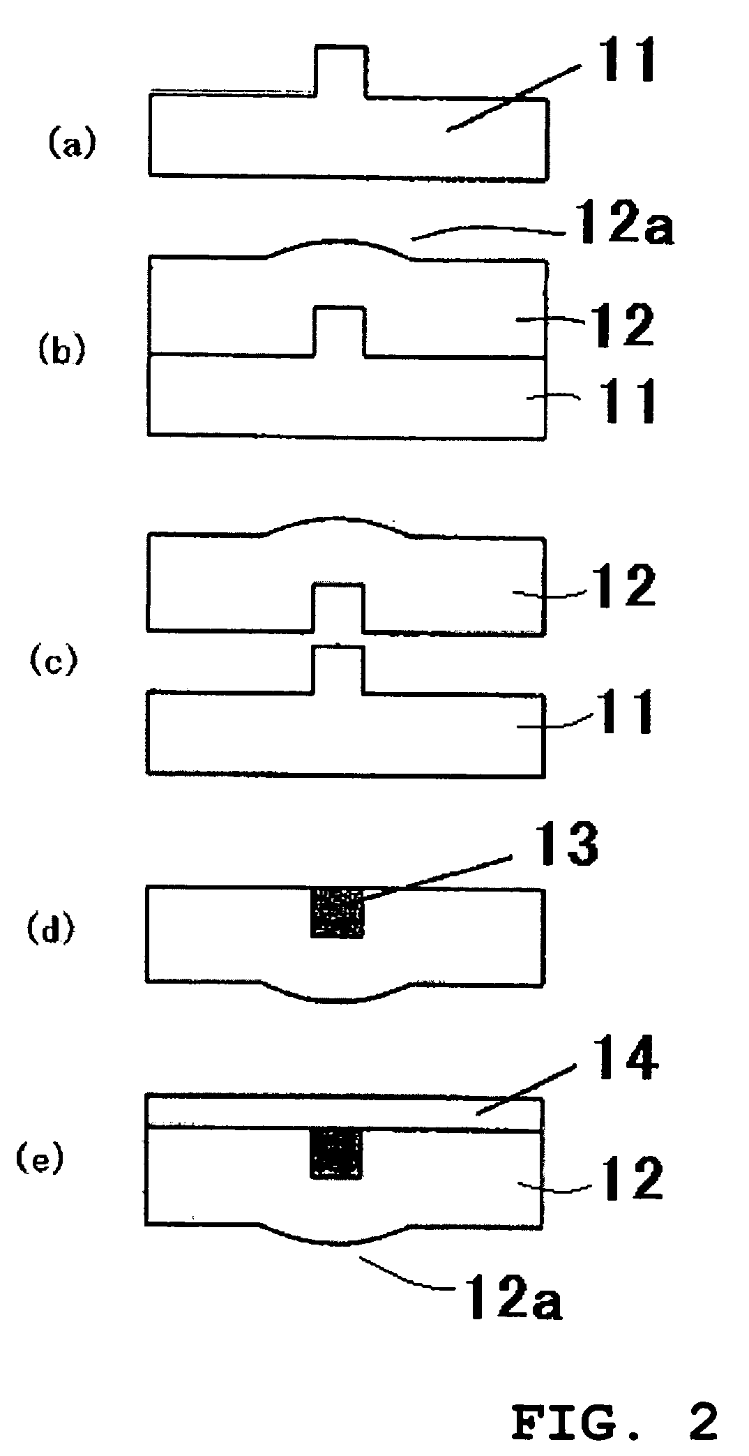
[0050]By dry-etching a 5-inch silicon wafer, a ridge-shaped core pattern having a width of 50 μm and a height of 40 μm is formed. This serves as a mold. A solution of poly(amic acid) including 2,2-bis(3,4-dicarboxy phenyl) hexafluoropropane 2 anhydride (6FDA) and 2,2-bis(trifluoro methyl)-4,4′-diaminobiphenyl (TFDB) is spin-coated thereon and is then made to be polyimide through heat treatment. At this time, the concentration of the solution of poly(amic acid) is set to 25%. A portion protruded along a core pattern is formed on the top surface of the cladding layer on the core pattern. Next, by immersing the cladding layer of polyimide in distilled water, the cladding layer is separated from the silicon wafer. Next, the formed groove is filled with co-polymerized polyimide including 6FDA, 4,4′-oxydianiline (ODA), and 6FDA / TFDB through spin coating and heat treatment. Further, a cladding layer made of 6FDA / TFDB is formed thereon. In this way, the film-shaped optical waveguide is form...

third embodiment

[0053]By forming the upper and lower cladding layers using polyimide including 2,2-bis(3,4-dicarboxy phenyl) hexafluoropropane 2 anhydride (6FDA) and 2,2-bis(trifluoro methyl)-4,4′-diaminobiphenyl (TFDB), forming the core layer using polyimide including 6FDA and 4,4′-oxydianiline (ODA), and performing the well-known methods of photolithography and dry etching thereto, a multimode optical waveguide film is formed on a 5-inch silicon wafer. At this time, the optical waveguide is patterned in a T shape. Thereafter, by immersing the silicon wafer, on which the optical waveguide is formed, in an aqueous solution of 5 wt % of hydrofluoric acid, the optical waveguide is separated from the silicon wafer, thereby forming a film-shaped optical waveguide. The thickness of the film-shaped optical waveguide is set to 80 μm.

[0054]Next, a rectangular through-hole is formed at the intersection of the T shape using a reduction optical system-mask projecting KrF excimer laser machining apparatus. The...


PUM


Abstract

An optical waveguide having means for performing optical coupling with high efficiency at a predetermined position in an optical circuit substrate and which optionally includes an optical-electrical circuit board. Also provided are an optical waveguide, an optical path thereof being changed in an optical circuit at a steep angle and the optical waveguide for performing coupling and splitting of light being decreased in size in the optical circuit. The optical waveguide has a core and a cladding layer, and a wall surface, which is formed by cutting out at least a part of the core in a thickness direction of the core through irradiation of a laser beam and crosses at least a part of the core, which is a specular surface.

Description

BACKGROUND OF THE INVENTION[0001]1. Field of the Invention[0002]The present invention relates to a polymer optical waveguide in which an optical path of a light beam can be changed, and more particularly, to a method of manufacturing an optical integrated circuit, an optical-interconnection optical component, an optical-electrical circuit board, etc.[0003]2. Description of the Related Art[0004]As base members of optical components or optical fibers, inorganic materials such as quartz glass or multi-element glass characterized by a low transmission loss and a wide transmission band are widely used. However, since recently developed polymer materials have excellent machining properties and low cost in comparison with these inorganic materials, the polymer materials have received a lot of attention as materials for optical waveguides. For example, there has been provided a flat optical waveguide having a core-clad structure in which a core is formed out of a polymer having excellent tr...

Claims


Application Information

Patent Timeline
Patent Type & Authority Patents(United States)
IPC IPC(8): G02B6/26G02B6/02G02B6/12G02B6/122G02B6/125G02B6/136G02B6/42
CPCG02B6/122G02B6/1221G02B6/125G02B6/136G02B2006/12176G02B6/4214G02B2006/12097G02B2006/12173G02B2006/12121
Inventor SHIODA, TSUYOSHISUZUKI, KENJI
Owner MITSUI CHEM INC
Learn More