Deposition method of insulating layers having low dielectric constant of semiconductor device, a thin film transistor substrate using the same and a method of manufacturing the same
a technology of insulating layers and semiconductor devices, applied in the direction of coatings, optics, instruments, etc., can solve the problems of increasing the difficulty of signal twisting due to an increase in various parasitic capacitances, increasing the cost of materials, and substantial loss, so as to improve the vapor deposition speed and reduce the process time , the effect of high aperture ratio structur
- Summary
- Abstract
- Description
- Claims
- Application Information
AI Technical Summary
Benefits of technology
Problems solved by technology
Method used
Image
Examples
examples 1 to 9
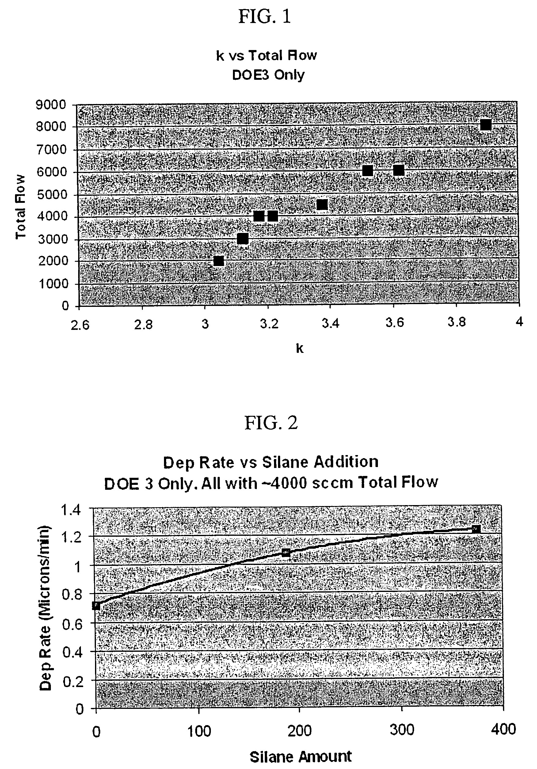
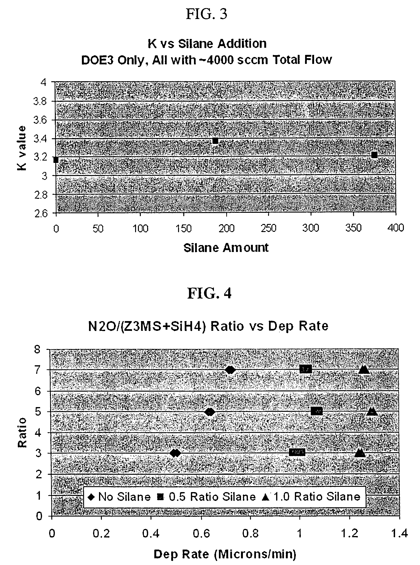
[0091]Using a capacitively coupled parallel plate PECVD reactor, a low dielectric insulating film was vapor deposited on a bare silicon wafer or glass substrate with a reactant gas mixture of trimethylsilane (3MS), silane (SiH4), nitrous oxide (N2O) and argon (Ar). A vapor deposition temperature was 270° C., and other parameters (i.e., dielectric constant and growth speed) for a PECVD process of the Examples are shown in Table 1.
[0092]Light transmittances for the insulating films formed on a glass substrate were measured. All showed a light transmittance of 95% or more at a wavelength range of 400 to 800 nm.
[0093]
TABLE 1TotalVaporflowdepositionElectricPressure3MSN2OArSiH4ratespeedpower(Torr)(sccm)(sccm)(sccm)(sccm)(sccm)(nm · min)KavgExam.115002.53751688750187.530001.0063.119215002.537528131100187.544751.083.375315002.537539381500187.560001.043.520415002.53752250100037540001.2483.216515002.53753750150037560001.2963.621615002.53755250200037580001.2663.897715002.53751125500020000.5063...
examples 10 to 14
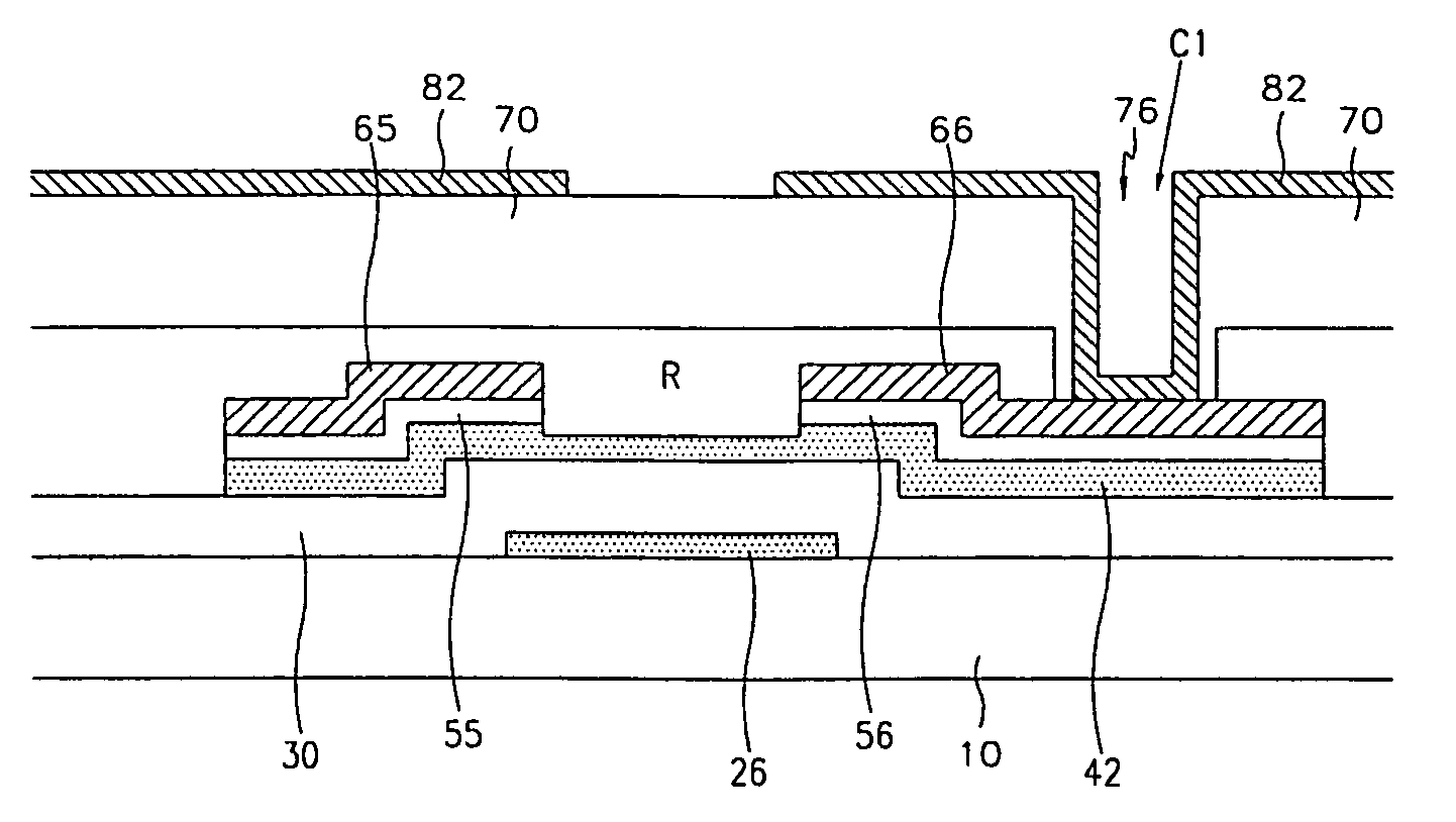
[0099]Referring to the attached figures, a thin film transistor substrate with a low resistance wiring structure according to the Examples of the present invention using the low dielectric insulating film as a protection film, and a preparation method thereof will be explained in detail. The explanation will be such that a person having ordinary knowledge in the art to which the present invention pertains can easily carry out the disclosure.
[0100]Referring to FIGS. 7 and 8, the structure of the thin film transistor substrate according to Example 10 of the present invention will be explained in detail.
[0101]FIG. 7 shows a thin film transistor substrate for a liquid crystal display according to Example 10 of the present invention, and FIG. 8 is a cross sectional view taken along line II-II of the thin film transistor substrate shown in FIG. 7.
[0102]On an insulating substrate (10), gate wiring comprised of double layers of first gate wiring layers (221, 241, 261) made of a Cr or Mo all...
PUM
| Property | Measurement | Unit |
|---|---|---|
| temperature | aaaaa | aaaaa |
| wavelength range | aaaaa | aaaaa |
| light transmittance | aaaaa | aaaaa |
Abstract
Description
Claims
Application Information
 - R&D Engineer
- R&D Manager
- IP Professional
- Industry Leading Data Capabilities
- Powerful AI technology
- Patent DNA Extraction
Browse by: Latest US Patents, China's latest patents, Technical Efficacy Thesaurus, Application Domain, Technology Topic, Popular Technical Reports.
© 2024 PatSnap. All rights reserved.Legal|Privacy policy|Modern Slavery Act Transparency Statement|Sitemap|About US| Contact US: help@patsnap.com


