3-D readout-electronics packaging for high-bandwidth massively paralleled imager

a massive parallel imager and readout technology, applied in the field of electronics component packaging, can solve the problems of complex and expensive hybrid approach of bonding the sensor chip to the roic cube as shown in fig. 1, affecting performance, packaging, complexity of the finished 3-d stack, etc., and achieve the effect of increasing the functionality per pixel

Inactive Publication Date: 2007-12-18
THE UNITED STATES AS REPRESENTED BY THE DEPARTMENT OF ENERGY
View PDF3 Cites 1 Cited by
  • Summary
  • Abstract
  • Description
  • Claims
  • Application Information

AI Technical Summary

Benefits of technology

[0008]According to unique embodiments of the present invention, “camera-on-a-chip” systems that increase the functionality per pixel through three-dimensional (3-D) stacking are possible. In accordance with features of the present invention, an array of photo-sensitive cells are disposed on a stacked CMOS ship's surface at a 45° degree angle from light reflecting mirror surfaces formed on a neighboring CMOS chip surface. Image processing electronics are held within the stacked CMOS chip layers. Electrical connections couple each of said stacked CMOS chip layers and a distribution grid, the connections for distributing power and signals to components associated with each stacked CSMO chip layer.
[0009]According to another feature of the present invention, the sophistication of co-integrated detector electronics is improved by permitting the merging of improved detection, signal conditioning, amplification, storage, digitization, and processing on a per-pixel basis over a large, dense array of detector pixels.
[0011]The methodologies described herein are superior to strictly monolithic and hybridized 2-D focal plane arrays, since in these existing 2-D schemes, it is necessary to confine the amount of electronics devoted to each pixel within the physical area corresponding to a single pixel unit cell. By using a 3-D methods as provided for and described herein, it is possible for those skilled in the art to greatly increase the effective area per unit pixel, which thereby permits a greater range of applications, including extremely fast imaging.
[0012]In accordance with benefits of the present invention, it is then possible to implement storage buffers, more sophisticated amplifiers, on-board processing facilities, and other circuitry so as to greatly extend the utility of these combined detector-electronics systems. This is possible because the amount of physical real estate for implementing electronics per pixel is greater. In previously described and practiced 3-D implementations, however, the means for achieving assemblies has been complicated, leading to complexities affecting the cost of constructing a practical assembly. The present invention circumvents the complexity disadvantage of previously demonstrated art in 3-D arrangements, while providing the essential advantages of a 3-D scheme.

Problems solved by technology

The hybrid approach of bonding the sensor chip to the ROIC cube as shown in FIG. 1 is complex and expensive.
Then the process of the lamination of the HDI layer, laser via drilling, bump deposition and bonding, is complex, expensive and can lead to reliability problems.
Each scheme can affect performance, packaging, and complexity of a finished 3-D stack.
This approach is simple, but has the primary disadvantage of requiring each substrate to have a slightly different length.
The two disadvantages are that: (1) a reliable means of forming and maintaining connections is required that does not cause shorting between the feedthroughs and the individual substrates and (2) the integrated circuit within each substrate must have the ability to arbitrate a unique identification within a given stack.

Method used


Image

  • 3-D readout-electronics packaging for high-bandwidth massively paralleled imager
  • 3-D readout-electronics packaging for high-bandwidth massively paralleled imager
  • 3-D readout-electronics packaging for high-bandwidth massively paralleled imager

Examples


Embodiment Construction

[0026]The purpose of the current invention is to inexpensively provide a means of increasing the functionality available in concepts related to “camera-on-a-chip” through a 3-D method. Described herein is an approach to reconcile the opposing demands for smaller, denser pixels and greater functionality.

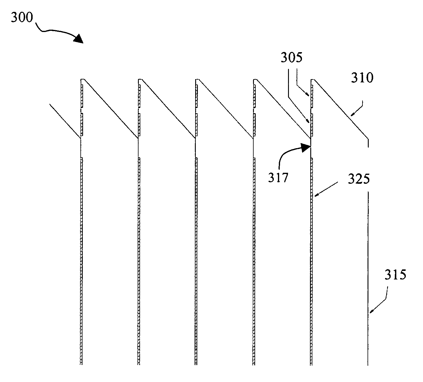
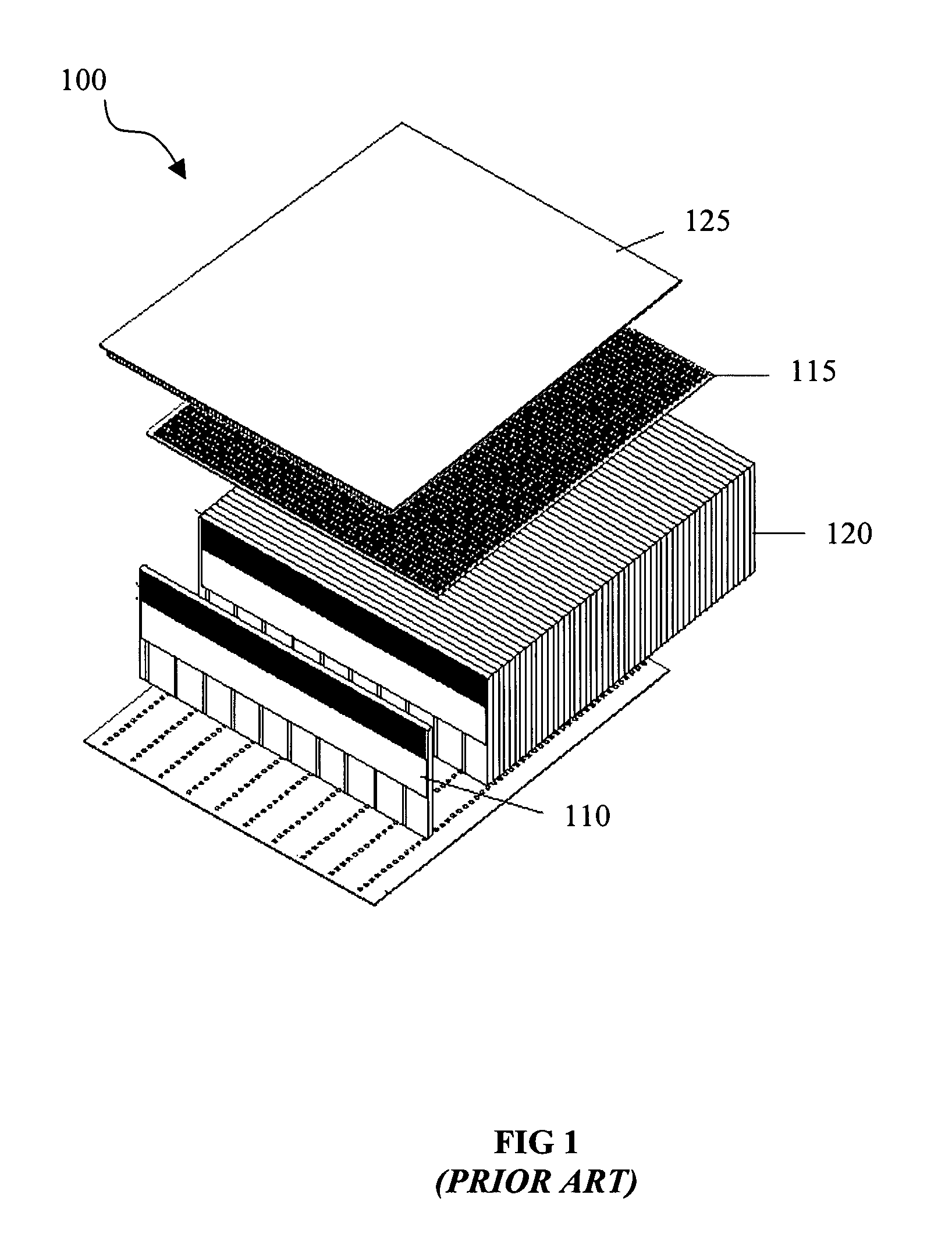
[0027]Referring to FIG. 1 (labeled “Prior Art”), a vertically stacked chip architecture 100 has been used to address complex electronic component interconnection problems. In this scheme, the readout integrated circuits (ROICs) 110 are stacked vertically (like playing cards) into a cube configuration 120. Another integrated circuit die 115, a fully depleted high-pixel photo-diode focal plane array (FPA), is bump bonded to the top edge surface of the resulting ROIC cube 120. The stacked cube edge footprint is contained within the X-Y dimensions of the photo-diode FPA die 125, so as to permit tiling a number of similar assemblies into large arrays. Input / output (I / O) from these cubes is...


PUM


Abstract

Dense, massively parallel signal processing electronics are co-packaged behind associated sensor pixels. Microchips containing a linear or bilinear arrangement of photo-sensors, together with associated complex electronics, are integrated into a simple 3-D structure (a “mirror cube”). An array of photo-sensitive cells are disposed on a stacked CMOS chip's surface at a 45° angle from light reflecting mirror surfaces formed on a neighboring CMOS chip surface. Image processing electronics are held within the stacked CMOS chip layers. Electrical connections couple each of said stacked CMOS chip layers and a distribution grid, the connections for distributing power and signals to components associated with each stacked CSMO chip layer.

Description

STATEMENT OF GOVERNMENT RIGHTS[0001]The United States Government has rights in this invention pursuant to Contract No. W-7405-ENG-36 between the United States Department of Energy and the University of California for the operation of the Los Alamos National Laboratory.FIELD OF THE INVENTION[0002]The present invention is generally related to electronics fabrication and electronics component packaging. More particularly, the present invention is related to improvements in 3-D electronics packaging and methods and means of efficiently joining monolithic pixel and electronic substrates into a 3-D array.BACKGROUND[0003]The construction of the 2-Mpixel, >32-frame, 200 ns imaging system is complicated by the tremendous requirements on data recording bandwidth, as well as by equally severe demands on the instantaneous power (ground) that has to be delivered to front-end electronics and sensor during acquisition. The bandwidth demands during processing imply that, for flash radiography, a...

Claims


Application Information

Patent Timeline
Patent Type & Authority Patents(United States)
IPC IPC(8): H01L29/04
CPCH01L27/14634H01L27/14618H01L2224/13H01L2224/32145H01L2224/48091H01L2224/73265H01L2225/06562H01L2924/10158H01L2924/00014
Inventor KWIATKOWSKI, KRISLYKE, JAMES
Owner THE UNITED STATES AS REPRESENTED BY THE DEPARTMENT OF ENERGY
Why Eureka
Try Eureka