
Three dimensional polymer memory cell systems

a memory cell and polymer technology, applied in semiconductor devices, semiconductor/solid-state device details, electrical devices, etc., can solve the problems of sensitivity to alignment tolerance, volatile memory cells usually lose information, and slowness of other types of storage devices, so as to facilitate the migration of charges and increase the amount of die space available for circuit design.

Inactive Publication Date: 2007-12-11
SPANSION LLC
View PDF3 Cites 29 Cited by
  • Summary
  • Abstract
  • Description
  • Claims
  • Application Information

AI Technical Summary

Benefits of technology

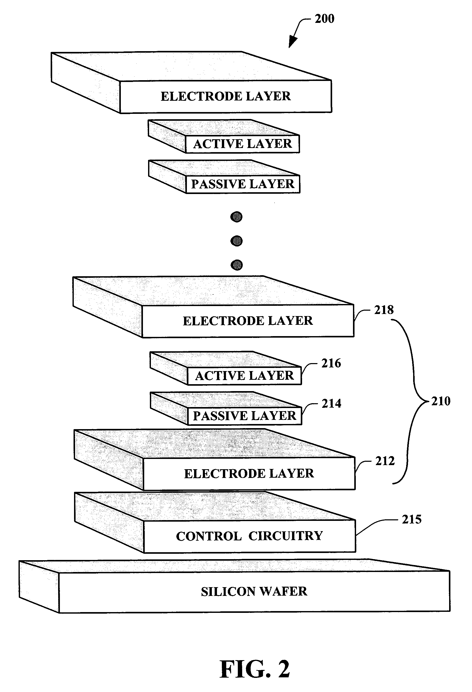
"The present invention provides systems and methods for creating three-dimensional memory structures using polymer memory cells. These cells are organized into a non-horizontal arrangement and can be programmed using a control component. The memory cells can include layers of alternating passive and active media, which facilitate the migration of charges to induce a desired programming state. The memory cells can be placed upon the control circuitry to program them. The invention also includes partitioning components that can separate the individual memory cells from each other. The invention allows for efficient placement of memory cells on a wafer surface and increases the amount of die space available for circuit design. The invention can be used in various applications such as data storage and memory devices."

Problems solved by technology

The long term storage mediums typically store larger amounts of information at a lower cost, but are slower than other types of storage devices.
Volatile memory cells usually lose their information if they lose power and typically require periodic refresh cycles to maintain their information.
Nonetheless, as the size of inorganic solid state devices decreases and integration increases, sensitivity to alignment tolerances can also increase making fabrication markedly more difficult.
Furthermore, such shrinkage for inorganic non-volatile memory cells, can be particularly difficult to do while maintaining low costs.
Accordingly, silicon-based devices are approaching their fundamental physical size limits, and further device shrinking and density increasing may be limited for such memory cells.

Method used


Image

  • Three dimensional polymer memory cell systems
  • Three dimensional polymer memory cell systems
  • Three dimensional polymer memory cell systems

Examples


Embodiment Construction

[0022]The present invention is now described with reference to the drawings, wherein like reference numerals are used to refer to like elements throughout. In the following description, for purposes of explanation, numerous specific details are set forth in order to provide a thorough understanding of the present invention. It may be evident, however, that the present invention may be practiced without these specific details. In other instances, well-known structures and devices are shown in block diagram form in order to facilitate describing the present invention.

[0023]Referring initially to FIG. 1, a perspective diagram of a system 100 is depicted, which is formed on a wafer surface 102, from blocks of individual polymer cells 110 positioned on top of each other to form stacked group 120. Such stacked group 120 can comprise N number of memory cells (N being an integer), programmable via control component (e.g. circuitry 105). Stacking memory cells according to the present inventi...


PUM


Abstract

Systems and methodologies are provided for forming three dimensional memory structures that are fabricated from blocks of individual polymer memory cells stacked on top of each other. Such a polymer memory structure can be formed on top of control component circuitries employed for programming a plurality of memory cells that form the stacked three dimensional structure. Such an arrangement provides for an efficient placement of polymer memory cell on a wafer surface, and increases amount of die space available for circuit design.

Description

TECHNICAL FIELD[0001]The present invention relates generally to memory cell group structures, and in particular to a three dimensional memory structure stack that groups polymer memory cell blocks together.BACKGROUND OF THE INVENTION[0002]The proliferation and increased usage of portable computer and electronic devices has greatly increased demand for memory cells. Digital cameras, digital audio players, personal digital assistants, and the like generally seek to employ large capacity memory cells (e.g., flash memory, smart media, compact flash, or the like). Memory cells can be typically employed in various types of storage devices. Storage devices include long term storage mediums such as, for example, hard disk drives, compact disk drives and corresponding media, digital video disk (DVD) drives, and the like. The long term storage mediums typically store larger amounts of information at a lower cost, but are slower than other types of storage devices. Storage devices also include...

Claims


Application Information

Patent Timeline
Patent Type & Authority Patents(United States)
IPC IPC(8): H01L23/58
CPCH01L25/0657H01L25/16H01L2924/3011H01L2924/0002H10K19/202H10K10/20H10K10/50H01L2924/00
Inventor MANDELL, AARONKRIEGER, JURI HSOKOLIK, IGORKINGSBOROUGH, RICHARD PSPITZER, STUART
Owner SPANSION LLC
Learn More