Silicon single crystal wafer, an epitaxial wafer and a method for producing a silicon single crystal

a single crystal, silicon technology, applied in the direction of polycrystalline material growth, after-treatment details, under protective fluid, etc., can solve the problems of oxide-film defects, degrading electrical characteristics, and degrading oxide dielectric breakdown voltage characteristic and device characteristics, so as to improve the yield of devices and excellent electrical characteristics and gettering ability

Active Publication Date: 2007-11-13
SHIN-ETSU HANDOTAI CO LTD
View PDF14 Cites 8 Cited by
  • Summary
  • Abstract
  • Description
  • Claims
  • Application Information

AI Technical Summary

Benefits of technology

[0016]An object of the present invention is to provide a silicon single crystal, which does not belong to any of V region rich in vacancy, OSF region and I region rich in interstitial silicon when producing the silicon single crystal by Czochralski method, has excellent electrical characteristics and gettering capability, and can surely improve yield of devices, and such an epitaxial wafer.

Problems solved by technology

In particular, there exist defects introduced during growth of a single crystal, called grown-in defects such as FPD, LSTD and COP, which degrade oxide dielectric breakdown voltage characteristic and device characteristics.
However, it has been found that there are some cases that oxide-film defects occur remarkably in spite of a single crystal wherein the N region occupies the entire plane, an OSF ring is not generated when thermal oxidation treatment is carried out, and FPD and L / D do not exist over the entire plane as mentioned above.
This may be a cause of degrading electrical characteristics such as oxide dielectric breakdown voltage characteristic.
Moreover, since dispersion of gettering capability occurs even if the crystals are grown in the above-described Nv region where the oxygen precipitation is large, yield of devices may not be necessarily improved.

Method used


Image

  • Silicon single crystal wafer, an epitaxial wafer and a method for producing a silicon single crystal
  • Silicon single crystal wafer, an epitaxial wafer and a method for producing a silicon single crystal
  • Silicon single crystal wafer, an epitaxial wafer and a method for producing a silicon single crystal

Examples


experiment 1

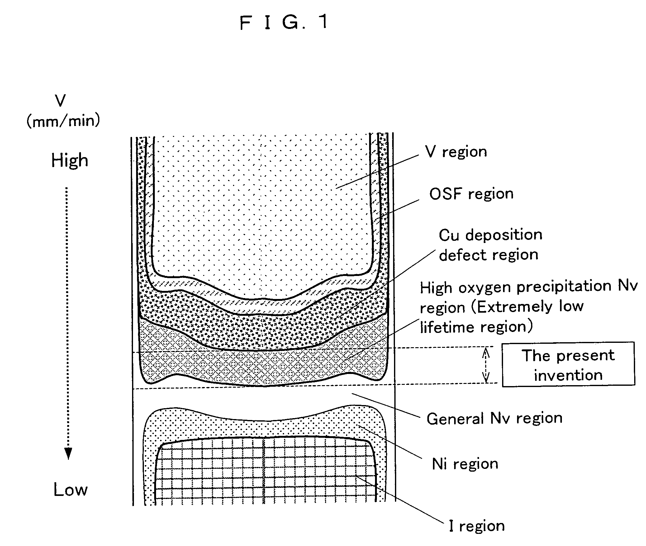
(Experiment 1): Confirmation of High Oxygen Precipitation Nv Region

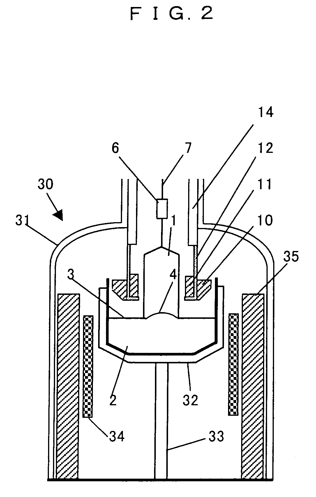
[0076]An experiment on gradual lowering of a crystal growth rate was carried out as explained below using the apparatus 30 for manufacturing a single crystal shown in FIG. 2 to research growth rates at boundaries of respective regions.

[0077]120 kg of polycrystalline silicon as a raw material was charged into a quartz crucible having a diameter of 24 inches (600 mm), and a silicon single crystal having a diameter of 8 inches (200 mm) and orientation of was grown. The single crystal was grown so that oxygen concentration in the wafer might be 24-27 ppma (ASTM+ 79 value). When growing the single crystal, the growth rate was controlled so as to gradually decrease linearly from 0.70 mm / min to 0.30 mm / min in a range from a point of 10 cm of a straight body through a tail.

[0078]The straight body of each silicon single crystal ingot grown as described above was cut into blocks by a length of 10 cm in the direction of a crys...


PUM

PropertyMeasurementUnit
sizeaaaaaaaaaa
diameteraaaaaaaaaa
melting pointaaaaaaaaaa

Abstract

In a method for producing a silicon single crystal by Czochralski method, the single crystal is grown with controlling a growth rate between a growth rate at a boundary where a defect region detected by Cu deposition remaining after disappearance of OSF ring disappears when gradually decreasing a growth rate of silicon single crystal during pulling and a growth rate at a boundary where a high oxygen precipitation Nv region having a density of BMDs of 1×10⁷ numbers / cm3 or more and / or a wafer lifetime of 30 μsec or less after oxygen precipitation treatment disappears when gradually decreasing the growth rate further. Thereby, there is provided a silicon single crystal which does not belong to any of V region rich in vacancy, OSF region and I region rich in interstitial silicon, and has excellent electrical characteristics and gettering capability, so that yield of devices can be surely improved, and also an epitaxial wafer.

Description

TECHNICAL FIELD[0001]The present invention relates to a silicon single crystal in N region having excellent electrical characteristics and gettering capability, in which any of defect regions such as V region, I region and OSF region as described below are not present and a defect region detected by Cu deposition does not exist either.BACKGROUND ART[0002]In recent years, in connection with miniaturization of devices accompanying higher integration of semiconductor circuits, a demand for quality of a silicon single crystal produced by Czochralski method (CZ method) which is used as a substrate thereof has been increasing. In particular, there exist defects introduced during growth of a single crystal, called grown-in defects such as FPD, LSTD and COP, which degrade oxide dielectric breakdown voltage characteristic and device characteristics. It has been considered that it is important to reduce a density and a size thereof.[0003]For explanation of these defects, there will be given f...

Claims


Application Information

Patent Timeline
Patent Type & Authority Patents(United States)
IPC IPC(8): C30B15/20C30B15/00C30B29/06H01L21/322
CPCC30B15/14C30B29/06C30B15/203H01L21/322
Inventor SAKURADA, MASAHIROMITAMURA, NOBUAKIFUSEGAWA, IZUMIOHTA, TOMOHIKO
Owner SHIN-ETSU HANDOTAI CO LTD
Why Eureka
Try Eureka