Clock generation circuit and clock generation method
a clock generation circuit and clock technology, applied in the direction of generating/distributing signals, pulse automatic control, electrical equipment, etc., can solve the problems of generating hazard before and after switching, generating spike noise, and conventional techniques do not teach any means to prevent such so as to improve the margin for stable operation of the clock generation circuit, prevent spike noise and hazard generation, and high accuracy
- Summary
- Abstract
- Description
- Claims
- Application Information
AI Technical Summary
Benefits of technology
Problems solved by technology
Method used
Image
Examples
first embodiment
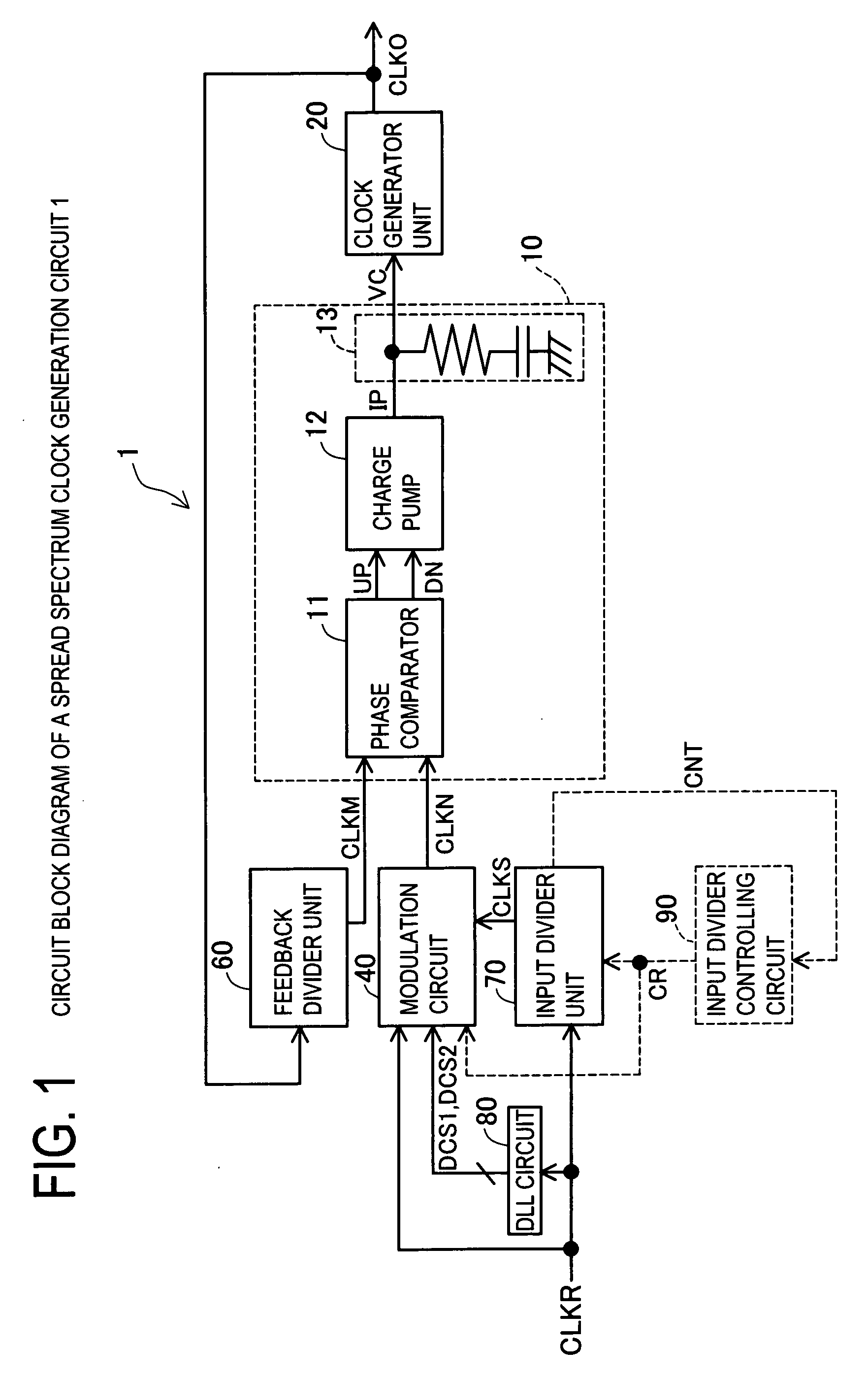
[0031]Next, reference will be made to FIGS. 4 to 6 to describe the operation of the spread spectrum clock generation circuit 1. The operation of the DLL circuit 80 will be explained. The delay circuit 82 delays the input clock signal CLKR and outputs the delay clock signal DLYCLK from the buffer of the last stage. The DLL control circuit 84 compares the phase of the input clock signal CLKR with the phase of the delay clock signal DLYCLK and controls the current values of the first current source unit 81 and the second current source unit 83 so as to make the phase difference between them equal to one cycle T0 (40 (ns)) of the input clock signal CLKR. That is, the DLL circuit 80 operates to make an adjustment so as to delay the phase of the delay clock signal DLYCLK from the input clock signal CLKR by one cycle T0. Thereby, the delay time for the buffer in each stage of the delay circuit 82 is made equal to the value obtained by dividing the cycle T0 by the number of buffer stages. I...
second embodiment
[0059]As fully described hereinabove, the spread spectrum clock generation circuit uses, for modulating the divided input clock signal CLKS, the first means for directly changing the cycle T1 of the divided input clock signal CLKS by changing the reload value CR of the input divider unit 70 and the second means for changing the cycle by sequentially selecting the delay clock signals CLKD1 to CLKD4 which are delayed from the divided input clock signal CLKS.
[0060]The minimum time of the modulation width obtained by the first means is equal to the cycle T0 (25 (ns)) of the input clock signal CLKR and therefore is sufficiently greater compared to the reference delay time tr=5 (ns) that is the minimum time of the modulation width obtained by the second means. Therefore, the modulation width can be arbitrarily set in increments of 5 (ns) through coarse adjustment of the modulation width in increments of 25 (ns) with the first means and fine adjustment of it in increments of 5 (ns) with t...
PUM
 Abstract
Description
Claims
Application Information
 - R&D
- Intellectual Property
- Life Sciences
- Materials
- Tech Scout
- Unparalleled Data Quality
- Higher Quality Content
- 60% Fewer Hallucinations
Browse by: Latest US Patents, China's latest patents, Technical Efficacy Thesaurus, Application Domain, Technology Topic, Popular Technical Reports.
© 2025 PatSnap. All rights reserved.Legal|Privacy policy|Modern Slavery Act Transparency Statement|Sitemap|About US| Contact US: help@patsnap.com


