Hetero-integrated strained silicon n- and p-MOSFETs

a technology of strained silicon and pmosfets, applied in the field of strained silicon nand pmosfets, can solve problems such as degrading device performan

Inactive Publication Date: 2007-09-25
GLOBALFOUNDRIES INC
View PDF6 Cites 3 Cited by
  • Summary
  • Abstract
  • Description
  • Claims
  • Application Information

AI Technical Summary

Benefits of technology

[0013]The inventive process has clear advantages over previous methods, including those described in U.S. Pat. No. 6,709,903. For instance, by changing the order of the SiGe layer growth and the implantation of He or other atom species, the number of process steps is reduced from 4 to 2 steps, where a step is defined as the use of a single tool. Furthermore, by doing the growth of the SiGe layer, the annealing and the subsequent semiconductor cap growth sequentially in a single tool, the cleanliness of the substrate surface is maintained and substrate cleaning steps needed after ion implantation and after annealing in a furnace in the previous method can be eliminated.
[0014]Thus, the inventive method considerably reduces the cost of fabricating these strained semiconductor substrates. In a first embodiment of the present invention, the entire wafer has the same layered structure. Thus, it is desirable that the biaxial compressive strain in the semiconductor cap be about 1% or greater, in order that the p-MOSFET performance is not degraded.
[0015]A further advantage of the inventive process is that in the case of a SiGe layer with low mismatch strain, i.e., less than about 1%, the degradation in p-MOSFET performance can be avoided by implanting He or other atoms only in the regions where the n-MOSFETS will be fabricated. Provided the SiGe layer is thin enough, negligible strain relaxation of the SiGe layer occurs in areas of the wafer that are not implanted. Thus in those areas the in-plane lattice parameter of the semiconductor cap is the same as that of the underlying unstrained Si-containing substrate and p-MOSFETs fabricated in these areas will have the same performance as those fabricated in a bulk Si or SOI substrate. Thus in this second embodiment of the present invention, wherein only areas where n-MOSFET will be fabricated are implanted, the inventive process not only reduces fabrication costs but also produces n-MOSFETs with enhanced performance while avoiding degradation of the p-MOSFETs.
[0016]However, it is also known that the performance of p-MOSFETs fabricated in SiGe under biaxial compressive strain is enhanced compared to p-MOSFETs of comparable dimension fabricated in Si. Therefore, in a third embodiment of this invention, the semiconductor cap is removed from the areas of the substrates that were not implanted and the p-MOSFET is fabricated in the compressively strained SiGe layer. Thus, p-MOSFETs with enhanced performance compared to those fabricated in unstrained Si are obtained in addition to n-MOSFETs with enhanced performance fabricated in a semiconducting material under biaxial tensile strain.
[0017]In a fourth embodiment of this invention, implantation of He or other atoms is done only in areas of the Si-containing substrate where the n-MOSFETs are to be fabricated and the strictly pseudomorphic or nearly pseudomorphic SiGe layer is grown selectively only in those same areas and not in other areas where the p-MOSFETs or other circuit components are to be fabricated. The embodiments described previously are restricted to SiGe layers that are sufficiently thin that no strain relaxation occurs in areas of the wafer that were not implanted. The fourth embodiment of the present invention permits the use of a thicker SiGe layer to obtain increased strain relaxation of the SiGe and thus a higher degree of biaxial tensile strain in the semiconductor cap. Because the SiGe layer is relatively thin (<0.5 μm), this embodiment of the present invention is not expected to cause serious problems for later device fabrication steps.

Problems solved by technology

The threading dislocations extend to the wafer surface where the devices are, and thus may degrade device performance.

Method used


Image

  • Hetero-integrated strained silicon n- and p-MOSFETs
  • Hetero-integrated strained silicon n- and p-MOSFETs
  • Hetero-integrated strained silicon n- and p-MOSFETs

Examples


first embodiment

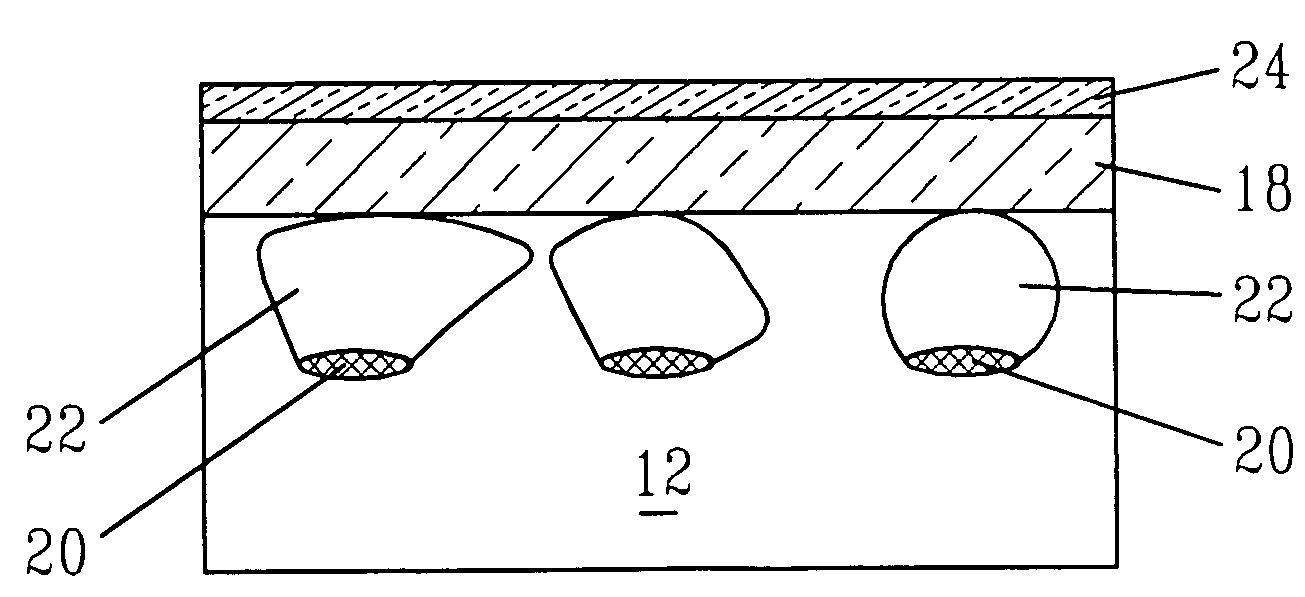
[0041]In the present invention, the light atoms are implanted across the entire area, i.e., surface, of the Si-containing substrate 12. The ion implant can be performed utilizing standard ion implant tools that are well known to those skilled in the art.

[0042]Next, and as shown in FIG. 4B, a strained SiGe alloy layer 16 is formed atop the surface of the Si-containing substrate 12 that includes the damaged region 14. By ‘strained’, it is meant that the SiGe alloy has a compressive or tensile stress associated therewith. The strained SiGe alloy layer is a nearly pseudomorphic or strictly pseudomorphic Si1−xGex material in which x (the mole fraction of Ge) is uniform and is from about 0.01 to about less than 1, preferably x is from about 0.15 to about 0.40, or a graded composition in which x increases from 0 at the surface of the Si-containing substrate 12 to higher x values (typically ranging from about 0.01 to less than about 1) at the upper regions of the SiGe alloy layer 16.

[0043]T...

fourth embodiment

[0062]the present invention is shown in FIGS. 7A-7D. This embodiment begins by providing the structure 50 shown in FIG. 7A. As shown, the structure 50 includes Si-containing substrate 12 having discrete and isolated damaged regions 14 located therein. The structure shown in FIG. 7A is the same as that shown in FIG. 5A; therefore the processing described above in regarding to FIG. 5A is applicable here for this embodiment of the present invention. Specifically, a masked ion implantation process is used to create the structure 50 shown in FIG. 7A.

[0063]Next, and as shown in FIG. 7B, areas of strained SiGe alloy 16 are selectively grown atop of the Si-containing substrate 12 in those regions that lay above the discrete and isolated damaged regions 14. The selective growth of strained SiGe alloy 16 can be achieved by either utilizing the same or different patterned mask as that used in forming the discrete and isolated damaged regions 14 within Si-containing substrate 12. The growth of ...

second embodiment

[0068]In the second embodiment, p-MOSFETs are fabricated atop the unstrained regions 56 of semiconductor layer 52, while n-MOSFETS are fabricating atop the strained regions 54 of semiconductor layer 52.


PUM

PropertyMeasurementUnit
temperatureaaaaaaaaaa
biaxial tensile strainaaaaaaaaaa

Abstract

The present invention provides semiconductor structures and a method of fabricating such structures for application of MOSFET devices. The semiconductor structures are fabricated in such a way so that the layer structure in the regions of the wafer where n-MOSFETs are fabricated is different from the layer structure in regions of the wafers where p-MOSFETs are fabricated. The structures are fabricated by first forming a damaged region with a surface of a Si-containing substrate by ion implanting of a light atom such as He. A strained SiGe alloy is then formed on the Si-containing substrate containing the damaged region. An annealing step is then employed to cause substantial relaxation of the strained SiGe alloy via a defect initiated strain relaxation. Next, a strained semiconductor cap such as strained Si is formed on the relaxed SiGe alloy.

Description

FIELD OF THE INVENTION[0001]The present invention relates to semiconductor structures and to methods of fabricating such structures for application for n- and p-metal oxide semiconductor field effect transistor (MOSFET) devices. More particularly, these semiconductor structures are fabricated in such a way so that the layer structure in the regions of the wafer where n-MOSFETs are fabricated is different from the layer structure in regions of the wafers where p-MOSFETs are fabricated. The present invention is also directed to a method for producing structures for the n-MOSFET including a Si-containing layer under biaxial tensile strain, which is the active region of the n-MOSFET, thus enhancing the device performance compared to a similar n-MOSFET fabricated on a standard bulk Si or Si-on-insulator (SOI) substrate.BACKGROUND OF THE INVENTION[0002]It is now well established that the performance of n-MOSFETs fabricated in a Si-containing layer under biaxial tensile strain is enhanced ...

Claims


Application Information

Patent Timeline
Patent Type & Authority Patents(United States)
IPC IPC(8): H01L21/265H01L21/00H01L21/84
CPCH01L21/02378H01L21/02381H01L21/02532H01L21/02664H01L21/26506H01L21/823807H01L29/1054H01L29/7842H01L21/26513Y10S438/938
Inventor BOYD, DIANE C.CAI, JUANCHAN, KEVIN K.MOONEY, PATRICIA M.RIM, KERN
Owner GLOBALFOUNDRIES INC
Why Eureka
Try Eureka