Semiconductor integrated circuit and liquid crystal display device

Active Publication Date: 2007-03-20
RENESAS ELECTRONICS CORP
View PDF5 Cites 23 Cited by
  • Summary
  • Abstract
  • Description
  • Claims
  • Application Information

AI Technical Summary

Benefits of technology

[0022]The semiconductor integrated circuit of the first aspect of the present invention is used as a signal line driving IC of a LCD device and the LCD device includes m pieces (“m” is a positive integer not less than 2) of signal line driving ICs and a LCD panel such that a first side of each of the m pieces of signal line driving ICs faces a side of the LCD panel in parallel therewith, along which side the input terminals of signal lines of the LCD panel are disposed, and CMADS bus output terminals of the i-th (“i” is a positive integer from 1 to m−1) signal line driving IC are connected to CMADS bus input terminals of the (i+1)-th signal line driving IC, the CMADS bus input terminals of the (i+1)-th signal line driving IC individually corresponding to the CMADS bus output terminals of the i-th signal line driving IC. Disposing and connecting the semiconductor integrated circuit of the present invention as described above allows the CMADS bus to substantially penetrate the inside of the semiconductor integrated circuit, thereby reducing a wiring area required for the second conventional example and further enhancing miniaturization of LCD device.
[0024]The semiconductor integrated circuit of the second aspect of the present invention is used as a signal line driving IC of a LCD device and the LCD device includes m pieces (“m” is a positive integer not less than 2) of signal line driving ICs and a LCD panel such that a first side of each of the m pieces of signal line driving ICs faces a side of the LCD panel in parallel therewith, along which side the input terminals of signal lines of the LCD panel are disposed, and CMADS bus output terminals of the i-th (“i” is a positive integer from 1 to m−1) signal line driving IC are connected to CMADS bus input terminals of the (i+1)-th signal line driving IC, the CMADS bus input terminals of the (i+1)-th signal line driving IC individually corresponding to the CMADS bus output terminals of the i-th signal line driving IC. Also in the second aspect of the present invention, since the CMADS bus is disposed to substantially penetrate the inside of the semiconductor integrated circuit, a wiring area required for the second conventional example can be eliminated and miniaturization of LCD device can further be enhanced.
[0027]The semiconductor integrated circuit of the third aspect of the present invention is used as a signal line driving IC of a LCD device and the LCD device includes m pieces (“m” is a positive integer not less than 2) of signal line driving ICs and a LCD panel such that a first side of each of the m pieces of signal line driving ICs faces a side of the LCD panel in parallel therewith, along which side the input terminals of signal lines of the LCD panel are disposed, and CMADS bus output terminals of the i-th (“i” is a positive integer from 1 to m−1) signal line driving IC are connected to CMADS bus input terminals of the (i+1)-th signal line driving IC, the CMADS bus input terminals of the (i+1)-th signal line driving IC individually corresponding to the CMADS bus output terminals of the i-th signal line driving IC. Also in the third aspect of the present invention, since the CMADS bus is disposed to substantially penetrate the inside of the semiconductor integrated circuit, a wiring area required for the second conventional example can be eliminated and miniaturization of LCD device can further be enhanced.
[0030]The semiconductor integrated circuit of the fourth aspect of the present invention is used as a signal line driving IC of a LCD device and the LCD device includes m pieces (“m” is a positive integer not less than 2) of signal line driving ICs and a LCD panel such that a first side of each of the m pieces of signal line driving ICs faces a side of the LCD panel in parallel therewith, along which side the input terminals of signal lines of the LCD panel are disposed, and CMADS bus output terminals of the i-th (“i” is a positive integer from 1 to m−1) signal line driving IC are connected to CMADS bus input terminals of the (i+1)-th signal line driving IC, the CMADS bus input terminals of the (i+1)-th signal line driving IC individually corresponding to the CMADS bus output terminals of the i-th signal line driving IC. Also in the fourth aspect of the present invention, since the CMADS bus is disposed to substantially penetrate the inside of the semiconductor integrated circuit, a wiring area required for the second conventional example can be eliminated and miniaturization of LCD device can further be enhanced.

Problems solved by technology

However, when producing high rate clock signals to transmit data at a higher rate, EMI (Electromagnetic Interference) occurs and the noise due to the EMI is imposed on the image data, adversely affecting quality of images to be displayed.
However, according to an ECL (Emitter Coupled Logic) interface, LVDS (Low Voltage Differential Signaling) interface or the like known as a conventional technique for providing a high rate interface while realizing low EMI, it is difficult to directly supply a signal from one transmitter to a plurality of receivers or it is required to most suitably and individually design the one transmitter depending on the number of the receivers and therefore, the conventional technique for providing a high rate interface has not easily been employed.
However, demand for a further miniaturized LCD device is growing and a high-resolution display device is strongly required to further reduce its volume.

Method used


Image

  • Semiconductor integrated circuit and liquid crystal display device
  • Semiconductor integrated circuit and liquid crystal display device
  • Semiconductor integrated circuit and liquid crystal display device

Examples


first embodiment

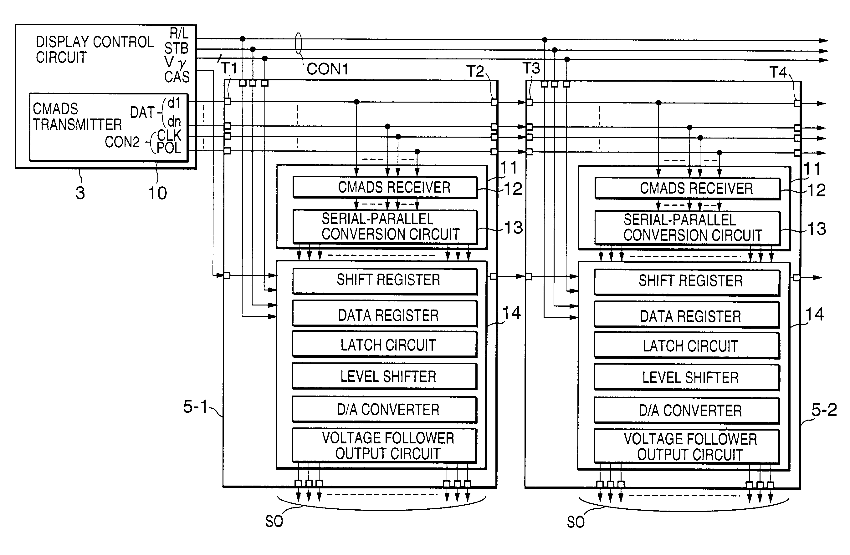
[0046]FIG. 5 is a schematic diagram illustrating internal blocks of the signal line driving IC 5, i.e., a semiconductor integrated circuit according to the present invention and a state of connection between the display control circuit and the signal line driving ICs adjacent thereto. Note that in FIG. 5, a CMADS transmitter 10 within a display control circuit 3 includes a plurality of the CMADS transmitters 81 shown in FIG. 3. The display control circuit 3 transmits a signal line control signal CON2 and image data DAT to the signal line driving IC 5-1 via a CMADS bus connected to the CMADS transmitter 10. In this case, the signal line control signal CON2 is a high rate signal including such as a clock signal CLK and a polarity inversion signal POL, and the image data DAT (including n pieces of data signals d1 to dn) is constructed such that parallel-serial conversion is made in units of a plurality of pixels with respect to image data representing gray scales of each of red, green ...

second embodiment

[0053]Referring to a diagram illustrating a disposition / connection layout of signal line driving ICs of FIG. 8A, an interface configuration of, the second embodiment will be explained. Image data DAT and a signal line control signal CON2 are transmitted from a CMADS transmitter 10 of a display control circuit 3 to a CMADS receiver 31 within a signal line driving IC 30-1 via a CMADS bus and amplified to have an amplitude of a CMOS signal equal to a power supply voltage VDD. When the signal received by the signal line driving IC 30-1 is a signal necessary for an internal circuit 14 of the IC 30-1, the signal is inputted to a serial-parallel conversion circuit 13. On the other hand, when the signal is a signal unnecessary for an internal circuit 14, the signal is again converted back to a signal of a CMADS signal amplitude by the CMADS transmitter 32 within the signal line driving IC 30-1 and then, the signal thus converted is transmitted as image data to a signal line driving IC 30-2 ...

third embodiment

[0057]An interface configuration of the third embodiment, will be explained. Image data DAT and a signal line control signal CON2 are transmitted to a signal line driving IC 40 via the CMADS bus and received by the first CMADS receiver 41a. The received data is again converted by the first CMADS transmitter 42a to a signal of a CMADS amplitude and then, transmitted via an internal CMADS bus within the signal line driving IC 40. When the data transmitted from the first CMADS transmitter 42a is data necessary for an internal circuit 14 of the signal line driving IC 40, the data is inputted to a third CMADS receiver 41c. On the other hand, when the data is data unnecessary for the internal circuit 14, the data is transmitted to the second CMADS receiver 41b located at the exit of the signal line driving IC 40. Subsequent to conversion of data by the first CMADS transmitter 42a, the data received by the second CMADS receiver 41b is converted again by the second CMADS transmitter 42b to ...


PUM


Abstract

A CMADS circuit is characterized in that one transmitter is able to drive a plurality of receivers at a high rate to make each of the receivers have a low amplitude. A signal line driving integrated circuit has input terminals formed along one side (for example, left side) of the integrated circuit for receiving each signal via each of CMADS bus lines and output terminals formed along an opposing side (right side) opposite the one side. The input and output terminals are disposed such that a distance from each of the input terminals to a side (lower side) of the integrated circuit along which the signal voltage output terminals are disposed becomes equal to that from each of the output terminals disposed to individually correspond to the input terminals to the lower side. Accordingly, a CMADS bus is formed penetrating the inside of the signal line driving integrated circuit. In a case where a CMADS bus couples a plurality of signal line driving integrated circuits in series, the CMADS bus signal lines constructed as described above can travel throughout a series of the signal line driving ICs without jackknifing at around connection portions between the adjacent integrated circuits, thereby substantially eliminating an entire part of a wiring area required for the conventional LCD device and realizing a small-sized LCD device.

Description

BACKGROUND OF THE INVENTION[0001]1. Field of the Invention[0002]The present invention relates to a semiconductor integrated circuit and a liquid crystal display device, and more particularly to a semiconductor integrated circuit for driving a source electrode of a TFT LCD panel and a liquid crystal display device comprised of a plurality of the semiconductor integrated circuits and the liquid crystal display panel.[0003]2. Description of Related Art[0004]FIG. 1 is a block diagram illustrating the configuration of a conventional liquid crystal display device (hereinafter, referred to as LCD device). In a LCD device 61, image data constituting an image signal and representing a degree of brightness of images at equal intervals on a logarithmic axis is employed as an input. A D.C. voltage varying in accordance with image data is generated based on a reference voltage within a LCD device and is supplied to a Liquid Crystal Display panel (LCD panel) 62 to display images. In this case, in...

Claims


Application Information

Patent Timeline
IPC IPC(8): G09G3/36G02F1/133G02F1/1345G09G3/20H01L21/822H01L27/04
CPCG09G3/3688G09G2370/08G09G2310/027G02F1/133
Inventor SUNOHARA, MAKOTO
Owner RENESAS ELECTRONICS CORP
Why Eureka
Try Eureka