
Method for manufacturing semiconductor chip

a technology of semiconductor chips and manufacturing methods, applied in the direction of optics, instruments, optical elements, etc., can solve the problems of difficult re-bonding of semiconductor wafers, difficult to handle after grinding, and difficult to re-bond semiconductor wafers without damage, etc., to achieve easy removal, easy and safer, and reduce the adhesion force of the adhesive layer

Inactive Publication Date: 2007-02-06
KANSAI PAINT CO LTD +1
View PDF3 Cites 13 Cited by
  • Summary
  • Abstract
  • Description
  • Claims
  • Application Information

AI Technical Summary

Benefits of technology

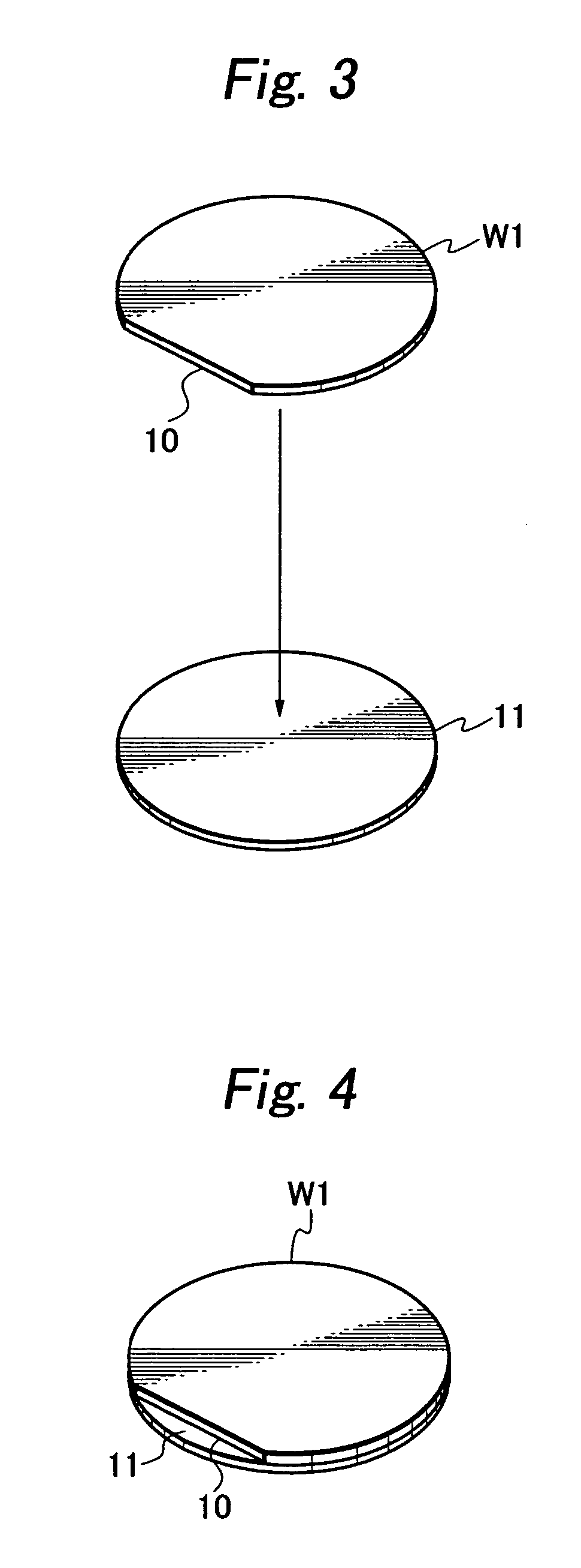
[0011]Meanwhile, the invention provides a method for manufacturing a semiconductor chip in which a semiconductor wafer, having a surface segmented by streets and formed with a plurality of circuits, is divided into circuit-based semiconductor chips, the method comprising: a groove forming step of resting a semiconductor wafer on a chuck table of a dicing apparatus and forming grooves in a front surface of the wafer to segment the plurality of circuits; a support substrate integrating step of bonding a front surface of the semiconductor wafer to a light-transmissive support substrate through an adhesive layer having an adhesion force that is reduced upon exposure to light radiation, thereby exposing a back surface of the semiconductor wafer; a grinding step of resting the semiconductor wafer integrated with the support substrate on a chuck table of a grinding apparatus and grinding the back surface of the semiconductor wafer into individual semiconductor chips until the grooves are exposed through the back surface of the wafer; a tape bonding step of bonding a tape on the back surface of the semiconductor wafer while the wafer is integrated with the support substrate after the grinding step and maintaining an outer shape of the semiconductor wafer, and supporting a periphery of the tape by a frame; and a re-bonding step of applying light radiation to the adhesive layer at a side close to the support substrate before or after the tape bonding step to thereby reduce an adhesion force of the adhesive layer, and removing the supporting substrate and adhesive layer from the front surface of the semiconductor wafer after the tape bonding step thereby supporting the semiconductor wafer by the tape and the frame.
[0019]In the method for manufacturing a semiconductor chip configured as described above, a semiconductor wafer is bonded to a rigid support substrate through an adhesive layer having an adhesion force that is reduced upon exposure to light radiation. In such a state, grinding is carried out to make the semiconductor wafer a desired thickness. Thereafter, light radiation is applied to the support substrate to thereby lower the adhesion force of the adhesive layer. Due to this, the semiconductor wafer or semiconductor chip is detached from the support substrate. Accordingly, the semiconductor wafer or semiconductor chips even if thinned can be easily removed without encountering damage.
[0020]Particularly, in the case that the adhesive layer is a liquid resin and the resin is formed of a composition of quinone-diazido compound and resin to foam and be reduced in adhesion force upon exposure to ultraviolet radiation, ultraviolet radiation is applied to the support substrate thereby concentrating a foaming region and forming a gap between the semiconductor wafer or semiconductor chips and the adhesive layer. Accordingly, detachment is made easier and safer from the support substrate.

Problems solved by technology

However, there is a setback that the thinned semiconductor wafer is as flexible as paper and hence is difficult to handle after grinding.
Because the ground semiconductor wafer is reduced in thickness, the semiconductor wafer, particularly ground to a thickness of 100 μm or smaller, or 50 μm or smaller, is readily damaged when detached from the support substrate and re-bonded onto a dicing tape.
Thus, there is a problem that it is difficult to re-bond a semiconductor wafer without causing damage.
In this case also, it is difficult to strip the semiconductor chips from the support substrate without causing damage.

Method used


Image

  • Method for manufacturing semiconductor chip
  • Method for manufacturing semiconductor chip
  • Method for manufacturing semiconductor chip

Examples


Embodiment Construction

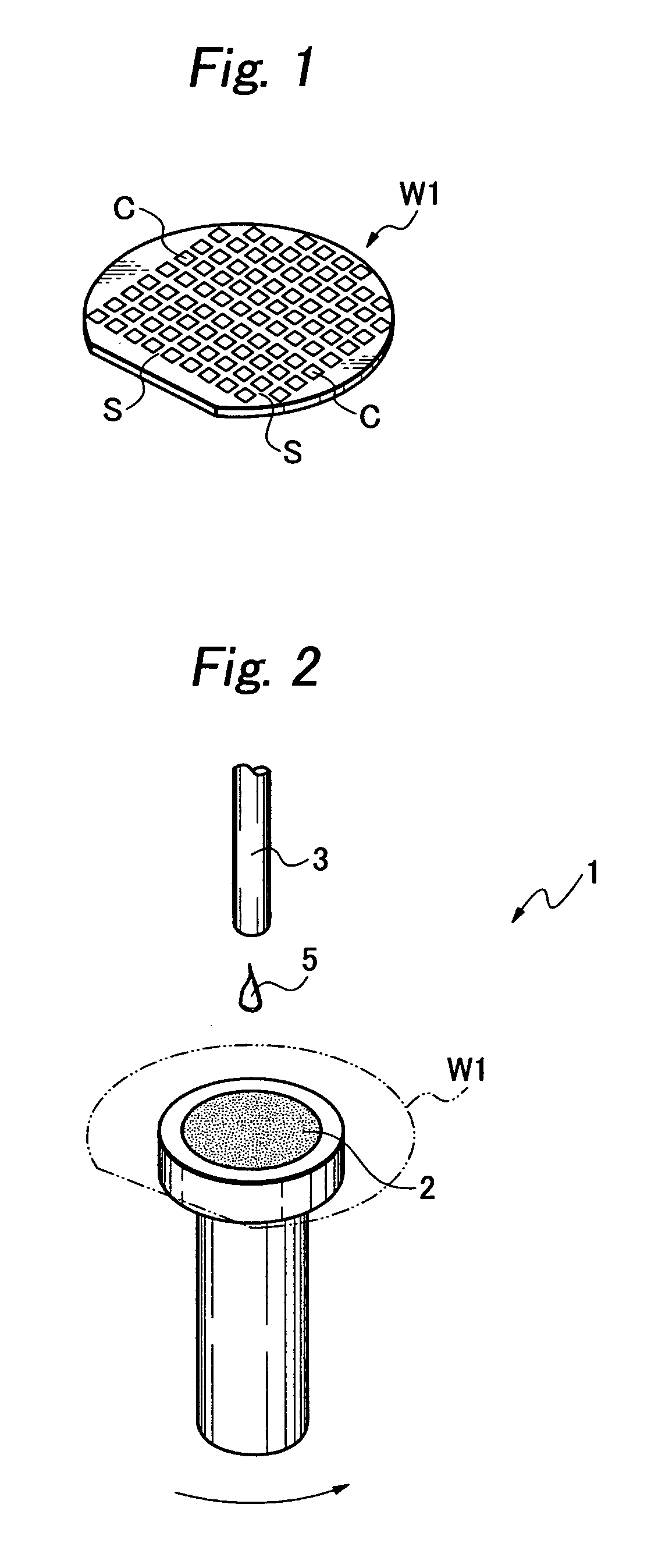
[0044]As an embodiment of the present invention, explanation is made of a method in which the semiconductor wafer W1, segmented by streets S and formed with a plurality of circuits C, is divided into individual semiconductor chips, as shown in FIG. 1.

[0045]At first, a spin coater 1, for example, shown in FIG. 2 is used, to coat an adhesive layer having an adhesion force that is reduced upon exposure to light, e.g. liquid resin adhesive layer 10, over the surface of a semiconductor wafer W1 or support substrate 11. The explanation herein is of a case in which liquid resin 5 is coated to the surface of the semiconductor wafer W1.

[0046]The spin coater 1 has at least a rotatable support table 2 and a drip part 3 for allowing liquid resin 10 to drip. The semiconductor wafer W1 is held face up on the support table 2. While the support table 2 is rotated at a rotation speed, for example, of 100–8000 rpm for 5 seconds or more, liquid resin is allowed to drip through the drip part 3, to carr...


PUM


Abstract

In manufacturing thinned semiconductor chips by grinding a semiconductor wafer supported on a rigid support substrate, in order to remove the semiconductor wafer or semiconductor chips from the support substrate without damage to the semiconductor wafer or semiconductor chips, a semiconductor wafer at its surface is bonded on a light-transmissive support substrate through an adhesive layer having an adhesion force that is reduced upon exposure to light radiation, thereby exposing the back surface of the semiconductor wafer. A tape is bonded to the backside of the semiconductor wafer integrated with the support substrate after grinding, wherein the tape is supported at the periphery. Before or after bonding of the tape, light radiation is applied to the adhesive layer at a side close to the support substrate to reduce the adhesion force in the adhesion layer. Thereafter, the support substrate and adhesive layer is removed from the surface of the semiconductor wafer, leaving the semiconductor wafer held by the tape and frame. The semiconductor wafer supported by the tape and frame is cut at streets into individual semiconductor chips.

Description

BACKGROUND OF THE INVENTION[0001]1. Field of the Invention[0002]The present invention relates to a method for manufacturing semiconductor chips while supporting a semiconductor wafer by use of a support substrate.[0003]2. Related Art[0004]The semiconductor wafer is formed with a plurality of circuits, such as ICs or LSIs. By dicing the wafer along streets on the surface thereof, the wafer is separated into a plurality of semiconductor chips that are to be used on a variety of electronic appliances.[0005]The semiconductor wafer is formed in a desired thickness by grinding at the back surface thereof. Recently, in order to reduce the size and weight of electronic appliances, the semiconductor wafer is necessarily worked to a thickness of 100 μm or smaller, or 50 μm or smaller.[0006]However, there is a setback that the thinned semiconductor wafer is as flexible as paper and hence is difficult to handle after grinding. For this reason, the semiconductor wafer is ground in a state bonded...

Claims


Application Information

Patent Timeline
Patent Type & Authority Patents(United States)
IPC IPC(8): H01L21/00H01L21/304H01L21/30H01L21/301H01L21/68H01L21/78
CPCH01L21/6835H01L21/6836H01L21/78H01L2221/6834H01L2221/68327G02B6/0065G02F1/1303G02F1/133524
Inventor TAKEZOE, KOUJIICHIKAWA, AKITOTAMURA, KOICHIKITAMURA, MASAHIKOYAJIMA, KOICHINANJO, MASATOSHINAMIOKA, SHINICHI
Owner KANSAI PAINT CO LTD
Learn More