
Shielded semiconductor chip carrier having a high-density external interface

a semiconductor chip and external interface technology, applied in the field of shielded, can solve the problems of large circuit board area occupied by conventional pga (pin grid array) packages, many deficiencies in conventional semiconductor packages,

Inactive Publication Date: 2006-11-14
ARIES ELECTRONICS
View PDF5 Cites 0 Cited by
  • Summary
  • Abstract
  • Description
  • Claims
  • Application Information

AI Technical Summary

Benefits of technology

This solution allows for a significantly smaller package size with increased signal speed and noise reduction, enabling more efficient and cost-effective semiconductor packaging that meets the demands of modern microprocessors by providing a high-density, pluggable, and SMT-compatible solution.

Problems solved by technology

Conventional semiconductor packages suffer from many deficiencies.
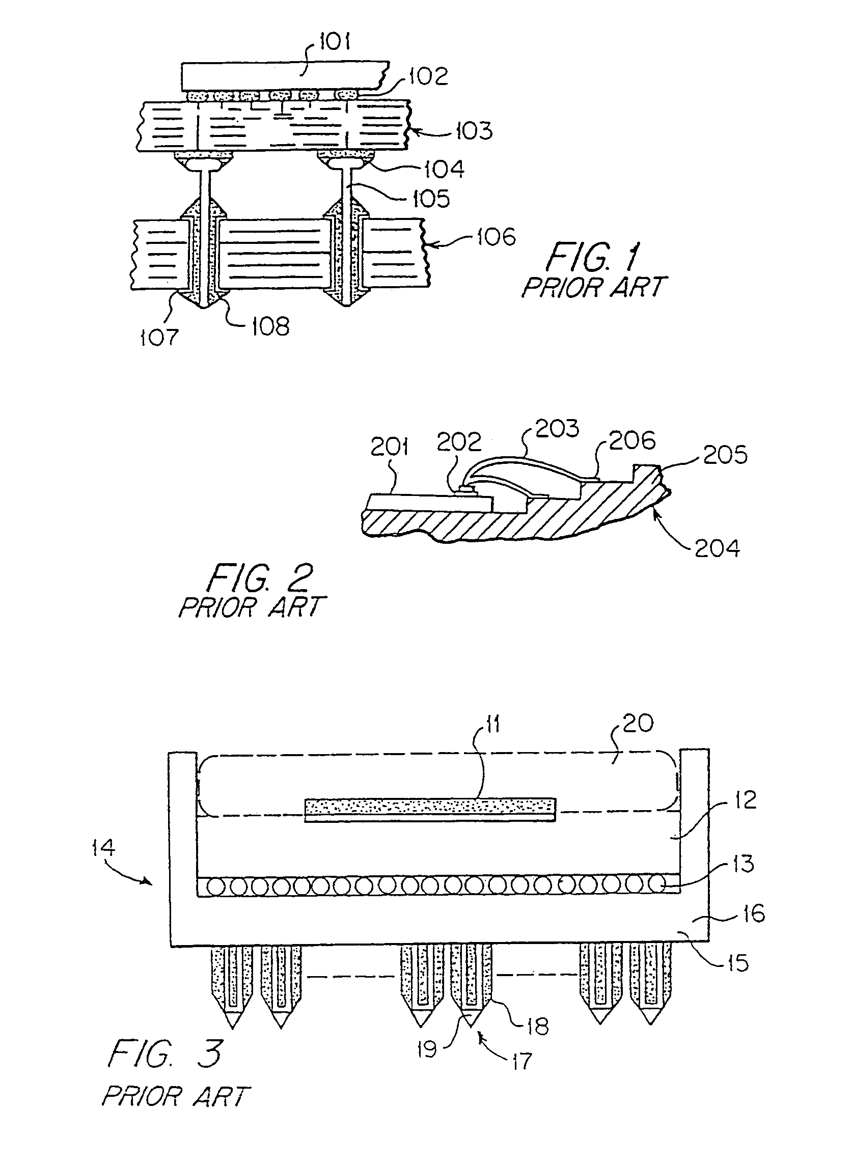
Conventional PGA (Pin Grid Array) packages, for example, tend to take up large amounts of circuit board area.
The manner in which conventional C4 and other bonding technologies are currently being used contributes to the aforementioned area usage problem.
For example, in C4 technology, the interconnections provide useful electrical connections, but do not provide an adequate amount of mechanical strength for the types of leads now in use.
Moreover, C4 connections are not typically applicable for use within pluggable semiconductor packages.
Moreover, the use of a multi-layer conductor for supporting the semiconductor die within the PGA package also adds to the size and cost of the PGA package.
Furthermore, conventional C4 bonding technology can result in problems with individual lead parasites, inspectability and testing problems, and problems relating to touch-up and repair of the connections.
These deficiencies include a lengthening in the amount of distance that electrical signals must travel within the semiconductor package, which lengthening affects signal propagation times; an increase in the amount of noise imparted to such electrical signals; an elevation in the power requirements for the semiconductor package; and an increase in the complexity of processes required to manufacture the semiconductor package.
Another problem associated with conventional PGA-type semiconductor packages is that such packages, when not used with a socket, are commonly mounted on PCBs using conventional plated-through hole technology.
This necessitates the performance of a soldering step, and such mounting technique increases the complexity and expense of the manufacturing operation.
Of course, the use of solder strictly limits upgradability of the assembly, thereby making it difficult to replace components.
The cost of the ceramic packaging material and brazed pin assembly is another disadvantage of PGA-type packages.
In addition, such packages have low-performance heat sink characteristics, and such packages are costly to manufacture because they include an excessive number of manufacturing processes.
Another problem associated with conventional semiconductor chip carriers relates to electrical interference.
From the foregoing, it can be understood that conventional semiconductor packages, such as PGA-type packages, take up large amounts of board space.
In addition, they are frequently not removably pluggable, and are not easily tested in the field or during manufacture.
It is common that such conventional semiconductor packages experience greater amounts of noise and have increased power requirements due to the long distances signals must travel within such packages.
As a result of the foregoing deficiencies incurred in semiconductor packaging technology, the latter is not sufficient to meet the needs of existing and / or future semiconductor and computer technology.

Method used


Image

  • Shielded semiconductor chip carrier having a high-density external interface
  • Shielded semiconductor chip carrier having a high-density external interface
  • Shielded semiconductor chip carrier having a high-density external interface

Examples


first embodiment

[0038]Turning to FIG. 5 which illustrates the subject invention, the pluggable aspects of the shielded semiconductor chip carrier 300 basically comprises plated printed circuit boards 302 and 310; blade contacts 320; and cooperating fork-like contacts 330.

[0039]The printed circuit board 302 is plated at its upper end 304, as well as having a plated-through hole 306. Similarly, printed circuit board 310 is plated on its lower end 312, and includes a plated-through hole 314, with the plating being provided for shielding purposes. Each blade contact 320 is elongated, and is molded at its upper end with a plastic bead material 322, with the distal end 324 of the blade being exposed for connection to a semiconductor die. Each blade contact 320 is maintained in the respective plated-through hole 306 by the press fit interference connection between the molded plastic material 322 and the plated-through hole 306 in such manner that the blade contact is spaced from, and hence electrically is...

second embodiment

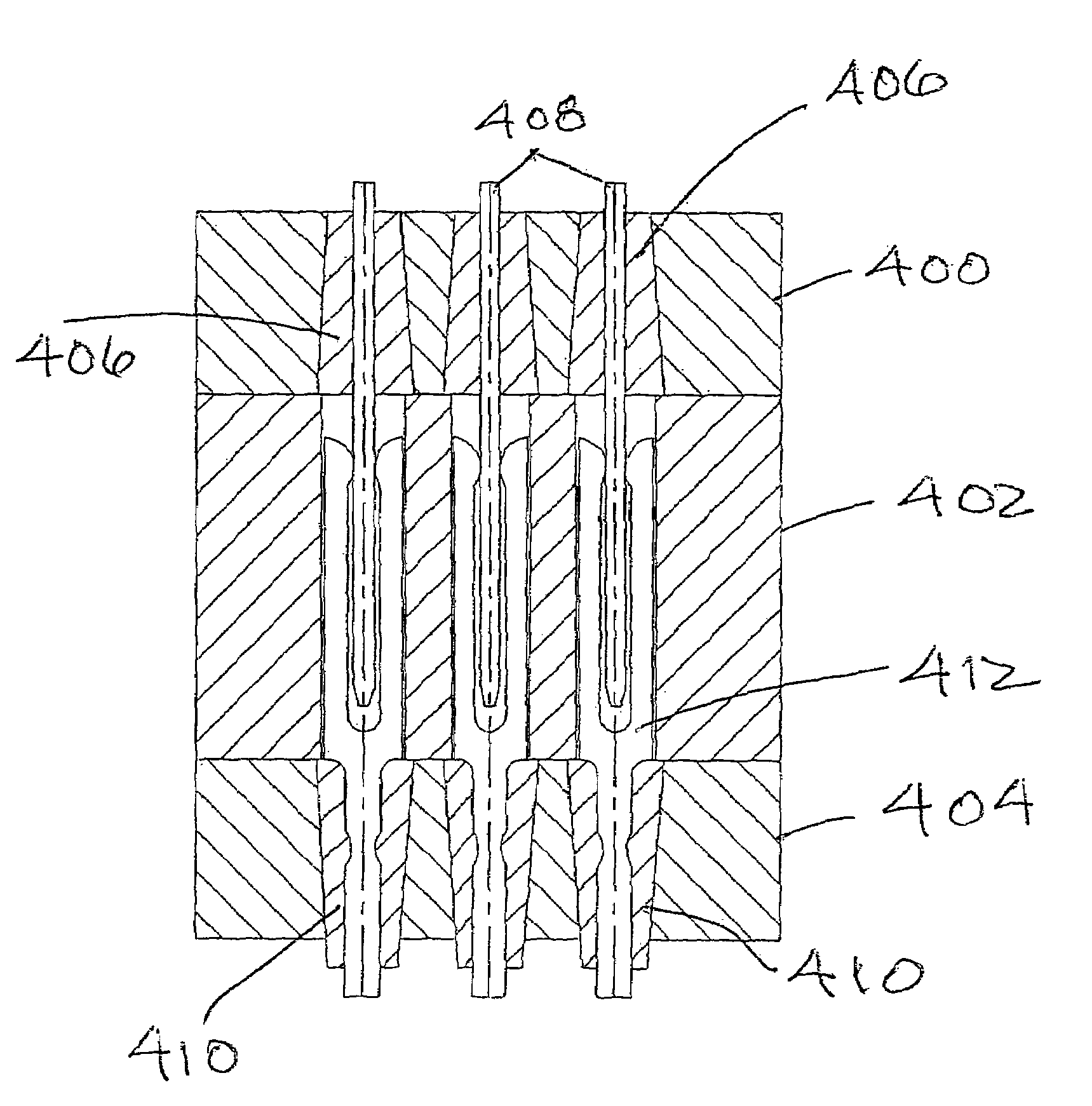
[0047]FIG. 6 is the pluggable aspects of the subject invention and is operationally similar to the embodiment of FIG. 5. As shown in FIG. 6, three printed circuit boards are employed, designated by the numerals 400, 402 and 404, each of which has a plated-through hole and with the upper and lower portions of the printed circuit boards also being plated for shielding purposes. The plastic bead 406 surrounding the blade 408 is tapered to facilitate insertion in an interference fit manner into the printed circuit board 400.

[0048]Likewise, the plastic material 410 molded to the fork-like contact 412 is tapered to facilitate the interference fit with the lower printed circuit board 404.

[0049]As in the case of the embodiment of FIG. 5, the interconnection between the blade 408 and the fork-like contact 412 occurs in the plated hole 414 extending through the central printed circuit board 402, with air (which is an excellent dielectric) surrounding the electrical interconnection.

[0050]In th...


PUM


Abstract

A shielded semiconductor chip carrier having a high-density external interface includes conventional printed circuit boards having plated through holes for achieving shielding of the contacts of the matrix. Two fork type connectors have molded about the distal ends thereof an annular ring of dielectric plastic material, and fork type connectors are press fit into each plated through hole, thereby locking the electrical contact within the shield formed by the plated through hole. The resulting connector provides a high-density contact matrix with each connector being electrically shielded along substantially its entire length.

Description

[0001]This application claims priority from U.S. Provisional Application No. 60 / 493,617, filed Aug. 7, 2003, which is incorporated herein by reference.BACKGROUND OF THE INVENTION[0002]1. Field of the Invention[0003]The present invention relates to a semiconductor chip or die carrier having a reduced size and, more particularly, a semiconductor die carrier affording an external interface having a high-density of electrically conductive contacts concentrated within a very small area and designed to shield the interconnection between the electrical contacts.[0004]2. Description of the Related Art[0005]Semiconductor packages typically contain a semiconductor die having bonding pads formed thereon, a plurality of leads connected to the bonding pads of the semiconductor die, and insulative packaging material formed around the semiconductor die and inner portions of the leads. Such a semiconductor package allows the transmission of electrical signals between the semiconductor die and an in...

Claims


Application Information

Patent Timeline
Patent Type & Authority Patents(United States)
IPC IPC(8): H01L23/552H01R12/16H01R13/11H01R13/115H05K5/00
CPCH01R23/6873H01R13/112H01R12/523H01L2224/16225H01R13/658
Inventor SINCLAIR, WILLIAM Y.
Owner ARIES ELECTRONICS
Learn More