Method for manufacturing semiconductor device having metal silicide

a technology of metal silicide and semiconductor devices, which is applied in the direction of semiconductor devices, electrical devices, transistors, etc., can solve the problems of high sheet resistance of source/drain, difficult to lower the sheet resistance, and greatly limited application field, so as to reduce the damage done to the boundary between the channel forming region and the source/drain region, the product yield can be improved, and the sheet resistance of the source/drain is high.

Inactive Publication Date: 2006-09-19
SEMICON ENERGY LAB CO LTD
View PDF113 Cites 27 Cited by
  • Summary
  • Abstract
  • Description
  • Claims
  • Application Information

AI Technical Summary

Benefits of technology

[0091]As described in the foregoing, the present invention provides a high performance TFT whose resistance between the channel forming region and the source / drain contacts is advantageously reduced by substantially shortening the distance therebetween. However, the advantage of the present invention is not only limited thereto. The sufficiently low resistance offers a reduced amount of impurities doped in the source / drain regions. More specifically, for example, a dose of 1×10¹⁵ to 8×1015 cm−2 generally required for impurity doping can be reduced by one digit or more, i.e., to a dose of 5×10¹³ to 1×1015 cm−2. Even with a lower dose of doped impurities, improved characteristics can be assured to the TFT obtained by the present invention. It can be seen by simple calculation that the doping step can be shortened to one tenth by employing the present invention.
[0092]Still advantageously, the damage done to the boundary between the channel forming region and the source / drain regions can be reduced by conducting impurity doping of low concentration. In a case the impurities are activated by laser annealing and the like, in particular, the degradation due to the impurities doped in a large concentration has been recognized as a serious problem because the gate contact and the like functioned as a shade to cause insufficient activation at the boundary between the channel forming region and the source / drain regions. An impurity doping of low concentration as in the present invention can effectively circumvent such a problem.
[0093]Furthermore, the active layer can be provided thinner. In a prior art process, it was difficult to reduce the thickness of the active layer to 1,000 Å or less, and more particularly, to 500 Å or less, because the sheet resistance of the source / drain was high. However, the TFT according to the present invention is free of such limitations. More specifically, a sheet resistance in the range of from 10 Ω to 1 kΩ can be realized for, e.g., a silicide layer 100 Å, because the resistivity thereof is as small as to fall within a range of from 10−3 to 10−5 Ω·cm.
[0094]A thinner active layer is advantageous not only in that it can be deposited within a shorter duration of film deposition, but also in that leak current and connection failure (step breakage) ascribed to insufficient step coverage of the gate insulator film and gate contact can be prevented from occurring. Conclusively, the product yield can be improved.

Problems solved by technology

An amorphous TFT using an amorphous material for the semiconductor film can also be fabricated; however, its application field is greatly limited because of its inferior operation speed ascribed to an extremely low mobility of 5 cm2 / Vs or even lower, about 1 cm2 / Vs in general, or because of its inability of providing a P-channel TFT (PTFT).
However, in a thermal process involving heating at a high temperature, in particular, only strictly selected substrate material can be used.
However, such a process requires long annealing, and moreover, the sheet resistance of the source / drain remains high due to insufficient activation of the impurities.
There is also an attempt of crystallizing the active layer and of activating source / drain by irradiating a laser beam and the like (this process is denoted as “laser process”, hereinafter), however, it has been found also difficult to lower the sheet resistance.
This problem may be solved by shortening the distance 74, however, this countermeasure is limited to a certain extent because too short a distance reversely impairs the precision upon matching the mask.
This is a serious problem particularly when a glass substrate is used, because shrinking of the glass substrate occurs during the heating steps (various types of annealing steps are indispensable) to give unfavorable results upon matching the mask.
Considering the problem of overetching upon forming contact holes connected to the source / drain regions, on the other hand, it is not possible to excessively shorten the distance 74.
As described in the foregoing, the conventional TFTs suffer the following disadvantages:(1) Problems are associated with the formation of contact holes connected to the source / drain regions; and(2) In view of the above problem (1), sheet resistance of the source / drain regions is also a problem because the contact hole cannot be located in the vicinity of the channel forming region.
Accordingly, a parasitic capacity which forms by the incorporation of the oxide layer 68 makes the operation unstable and lowers the reliability of the TFT.
However, since the thickness of the oxide layer 68 corresponds to the length of the offset gate, the thickness thereof can not be simply increased as desired.
At any rate, this type of TFT is not practically feasible.
Moreover, the damage of the active layer and the gate insulator film 1304 increases with increasing concentration of the doped impurities.
However, the accelerated ions contain a plurality atoms such as of hydrogen to result in a heat up of the substrate.
This problem becomes particularly distinct with increasing density of the plasma.
Accordingly, problems occur upon doping, including heating up of the device and thereby damaging it, and, in case a photoresist is used, carbonizing it and thereby making its removal difficult.
Concerning the measure (2) above, too intense an energy not only causes peeling off of the active layer or the gate contact and thereby lowering the yield of the TFT, but also impairs the throughput.
In using a laser, for instance, it is necessary to intensely converge the beam to increase the energy density, because the energy itself cannot be greatly intensified.
This inevitably decreases the beam area, and the treatment hence requires a longer duration of irradiation to cover an area of the same size.
This is a serious problem particularly when a glass substrate is used, because shrinking of the glass substrate occurs during the heating steps (various types of annealing steps are indispensable in the process) to give unfavorable results upon matching the mask.
As described in the foregoing, it is next to impossible to further lower the parasitic resistance of the source / drain regions so long a prior art process is employed.

Method used


Image

  • Method for manufacturing semiconductor device having metal silicide
  • Method for manufacturing semiconductor device having metal silicide
  • Method for manufacturing semiconductor device having metal silicide

Examples


example 1

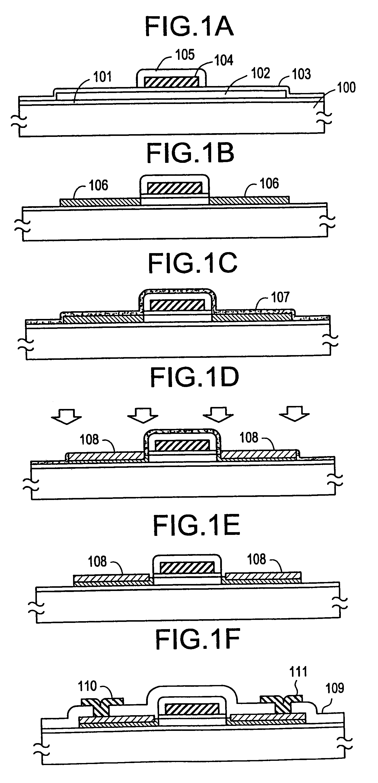
[0096]Referring to FIG. 1, a process for fabricating a TFT according to an embodiment of the present invention is described below. A 100 to 300 nm thick silicon oxide film 101 was deposited by sputtering in oxygen atmosphere as a base oxide film on a Corning 7059 substrate 100 (300 mm×460 mm in size or 100 mm×100 mm in size). As a process more suited for mass production, however, the base oxide film may be formed by decomposing and depositing TEOS (tetraethoxysilane) using plasma CVD, and annealing the resulting film at a temperature in the range of from 450 to 650° C.

[0097]Then, an amorphous silicon film was deposited by plasma CVD or LPCVD to a thickness of from 30 to 500 nm, preferably from 100 to 300 nm, and was allowed to stand in a reducing atmosphere for 24 hours at a temperature of from 550 to 600° C. to effect crystallization. This step may be performed by laser irradiation. The resulting crystallized silicon film was patterned to give island-like portion 102. A silicon oxi...

example 2

[0105]Referring to FIG. 2, a process for fabricating a TFT according to an embodiment of the present invention is described below. Thus, a base oxide film 202, an island like semiconductor region, and a silicon oxide film which functions as a gate oxide film 204 were formed on a Corning 7059 substrate 100 sequentially in the same manner as in Example 1. Then, a gate contact 205 was formed from an aluminum film from 200 nm to 5 μm in thickness. As shown in FIG. 2(A), an impurity region 203 was formed by implanting impurities using the gate contact as the mask.

[0106]An anodic oxide 206 was then formed around the gate contact (i.e., on the sides and the upper surface of the gate contact) by anodic oxidation in the same manner as that used in Example 1. It should be noted, however, that the impurity region far intrudes into the inner of the anodic oxide as compared to the case of Example 1. Subsequently, the surface of the impurity region was exposed by removing the silicon oxide film e...

example 3

[0109]Referring to FIG. 3, a process for fabricating a TFT according to an embodiment of the present invention is described below. Referring to FIG. 3(A), a base oxide film 301, an island like semiconductor region 302, a silicon oxide film which functions as a gate oxide film 303, and an aluminum film from 200 nm to 5 μm in thickness as a gate contact 304 were formed on a Corning 7059 substrate 300 sequentially in the same manner as in Example 1 above. Then, an anodic oxide 305 was formed on the periphery (the sides and the upper surface) of the gate contact by anodic oxidation following the same procedure as in Example 1.

[0110]Then, the silicon oxide film 303 was removed except for the portion under the contact portion, and a 5 to 50 nm thick platinum (Pt) film 306 was deposited by sputtering to obtain a structure shown in FIG. 3(B). Impurities were introduced through the platinum film by ion doping to obtain an impurity region 307 as shown in FIG. 3(C). Subsequently thereafter, th...


PUM


Abstract

A thin film transistor device reduced substantially in resistance between the source and the drain by incorporating a silicide film, which is fabricated by a process comprising forming a gate insulator film and a gate contact on a silicon substrate, anodically oxidizing the gate contact, covering an exposed surface of the silicon semiconductor with a metal, and irradiating an intense light such as a laser beam to the metal film either from the upper side or from an insulator substrate side to allow the metal coating to react with silicon to obtain a silicide film. The metal silicide layer may be obtained otherwise by tightly adhering a metal coating to the exposed source and drain regions using an insulator formed into an approximately triangular shape, preferably 1 μm or less in width, and allowing the metal to react with silicon.A high performance TFT can be realized. The metal silicide layer achieves favorable contact with the source and the drain, and, since it has a lower resistivity than silicon, the parasitic resistance between the source and drain regions can be considerably lowered.

Description

BACKGROUND OF THE INVENTION[0001]1. Field of the Invention[0002]The present invention relates to a structure of a thin film transistor (TFT) and to a process for fabricating the same. The present invention also relates to a process for fabricating an insulated gate semiconductor device on an insulator substrate and to a process for fabricating an integrated circuit (IC) obtained by assembling a plurality of said insulated gate semiconductor devices on an insulator substrate. The term “insulator substrate” as referred herein means any article having an insulating surface, and, if not particularly stated, it encompasses not only those made of insulating materials such as glass, but also articles having thereon an insulator layer and made of a material such as a semiconductor and a metal. The semiconductor device according to the present invention is useful as TFTs of active matrices of liquid crystal displays, driver circuits of image sensors, or SOI (silicon on insulator) integrated ...

Claims


Application Information

Patent Timeline
Patent Type & Authority Patents(United States)
IPC IPC(8): H01L21/4763H01L21/336H01L21/70H01L21/77H01L21/84H01L27/12H01L29/45H01L29/49H01L29/772H01L29/78H01L29/786
CPCH01L27/12H01L29/458H01L29/4908H01L27/124H01L29/78621H01L29/78696H01L29/66757Y10S257/90H01L21/18H01L29/78
Inventor TAKEMURA, YASUHIKOZHANG, HONGYONGTERAMOTO, SATOSHI
Owner SEMICON ENERGY LAB CO LTD
Why Eureka
Try Eureka